SLOS431B March 2004 – February 2015 TPA6120A2
PRODUCTION DATA.
- 1 Features
- 2 Applications
- 3 Description
- 4 Simplified Schematic
- 5 Revision History
- 6 Pin Configuration and Functions
- 7 Specifications
- 8 Parameter Measurement Information
- 9 Detailed Description
- 10Applications and Implementation
- 11Power Supply Recommendations
- 12Layout
- 13Device and Documentation Support
- 14Mechanical, Packaging, and Orderable Information
Package Options
Refer to the PDF data sheet for device specific package drawings
Mechanical Data (Package|Pins)
- RGY|14
- DWP|20
Thermal pad, mechanical data (Package|Pins)
Orderable Information
1 Features
2 Applications
- Professional Audio Equipment
- HiFi Smartphone
- Consumer Home Audio Equipment
- Headphone Drivers
3 Description
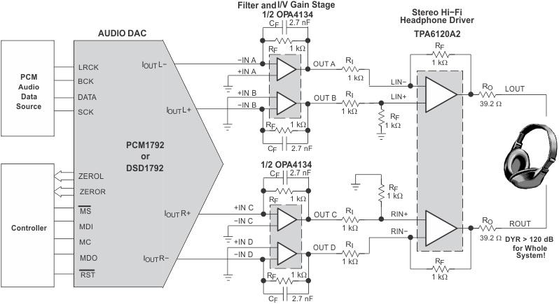
In applications requiring a high-power output, very high fidelity headphone amplifier, the TPA6120A2 replaces a costly discrete design and allows music, not the amplifier, to be heard. The TPA6120A2's current-feedback AB amplifier architecture delivers high bandwidth, extremely low noise, and up to 128dB of dynamic range.
Three key features make current-feedback amplifiers outstanding for audio. The first feature is the high slew rate that prevents odd order distortion anomalies. The second feature is current-on-demand at the output that enables the amplifier to respond quickly and linearly when necessary without risk of output distortion. When large amounts of output power are suddenly needed, the amplifier can respond extremely quickly without raising the noise floor of the system and degrading the signal-to-noise ratio. The third feature is the gain-independent frequency response that allows the full bandwidth of the amplifier to be used over a wide range of gain settings.
Device Information(1)
| PART NUMBER | PACKAGE | BODY SIZE (NOM) |
|---|---|---|
| TPA6120A2 | HSOP (20) | 7.5mm x 12.82mm |
| VQFN (14) | 3.5mm x 3.5mm |
- For all available packages, see the orderable addendum at the end of the datasheet.
4 Simplified Schematic