SLVSC89A June   2014  – July 2014 TSC2013-Q1

PRODUCTION DATA.  

  1. Features
  2. Applications
  3. Description
  4. Revision History
  5. Pin Configurations and Functions
  6. Specifications
    1. 6.1  Absolute Maximum Ratings
    2. 6.2  Handling Ratings
    3. 6.3  Recommended Operating Conditions
    4. 6.4  Thermal Information
    5. 6.5  Electrical Characteristics
    6. 6.6  Timing Requirements — I2C Standard Mode (ƒ(SCL) = 100 kHz)
    7. 6.7  Timing Requirements — I2C Fast Mode (ƒ(SCL) = 400 kHz)
    8. 6.8  Timing Requirements — I2C High-Speed Mode (ƒ(SCL) = 1.7 MHz)
    9. 6.9  Timing Requirements — I2C High-Speed Mode (ƒ(SCL) = 3.4 MHz)
    10. 6.10 Typical Characteristics
  7. Detailed Description
    1. 7.1 Overview
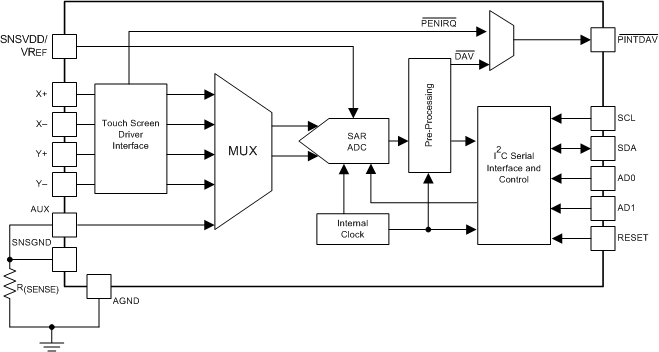
    2. 7.2 Functional Block Diagram
    3. 7.3 Feature Description
      1. 7.3.1 Touch-Screen Operation
      2. 7.3.2 4-Wire Touch Screen Measurements
      3. 7.3.3 Analog-to-Digital Converter
        1. 7.3.3.1 Data Format
        2. 7.3.3.2 Reference
        3. 7.3.3.3 Variable Resolution
        4. 7.3.3.4 Conversion Clock and Conversion Time
        5. 7.3.3.5 Touch Detect
        6. 7.3.3.6 Preprocessing
          1. 7.3.3.6.1 Preprocessing—Median Value Filter and Averaging Value Filter
    4. 7.4 Device Functional Modes
      1. 7.4.1 Conversion Controlled by TSC2013-Q1 and Initiated by TSC2013-Q1 (TSMode 1)
        1. 7.4.1.1 IX-IY Scan
        2. 7.4.1.2 X-Triplet, Y-Triplet, Z-Scan
      2. 7.4.2 Conversion Controlled by TSC2013-Q1 and Initiated by Host (TSMode 2)
      3. 7.4.3 Conversion Controlled by Host (TSMode 3)
    5. 7.5 Programming
      1. 7.5.1 I2C Interface
        1. 7.5.1.1 I2C Fast or Standard Mode (F-S Mode)
        2. 7.5.1.2 I2C High-Speed Mode (Hs Mode)
      2. 7.5.2 Digital Interface
        1. 7.5.2.1 Address Byte
      3. 7.5.3 Control Byte
        1. 7.5.3.1 Touch-Screen Scan Function for XYZ or XY
      4. 7.5.4 Start a Write Cycle
      5. 7.5.5 Register Access
      6. 7.5.6 Communication Protocol
      7. 7.5.7 Register Reset
    6. 7.6 Register Maps
      1. 7.6.1 Register Content and Reset Values
      2. 7.6.2 Configuration and Status Registers
        1. 7.6.2.1 Configuration Register 0
          1. 7.6.2.1.1 Configuration Register 0 (address = 0) [reset = 4000h for read; 0000h for write]
        2. 7.6.2.2 Configuration Register 1 (address = Dh) [reset = 0000h]
        3. 7.6.2.3 Configuration Register 2 (address = Eh) [reset = 0000h]
        4. 7.6.2.4 Converter-Function Select Register (address = Fh) [reset = 0000h]
        5. 7.6.2.5 Status Register (address = 8h) [reset = 0004h]
      3. 7.6.3 Data Registers
        1. 7.6.3.1 X1, X2, IX, Y1, Y2, IY, Z1, Z2, and AUX registers (offset = see ) [reset = see ]
  8. Application and Implementation
    1. 8.1 Application Information
      1. 8.1.1 Auxiliary Measurement
      2. 8.1.2 Single IX or Single IY Measurement
    2. 8.2 Typical Application
      1. 8.2.1 Design Requirements
      2. 8.2.2 Detailed Design Procedure
        1. 8.2.2.1 Power-On-Reset and Reset Consideration
          1. 8.2.2.1.1 Power-On Reset
          2. 8.2.2.1.2 Requesting a Minimal t(SNSVDD_OFF) Time
          3. 8.2.2.1.3 Requesting a Minimal t(SNSVDD_OFF_ramp) and t(SNSVDD_ON_ramp) Ramp
          4. 8.2.2.1.4 Hardware Reset
          5. 8.2.2.1.5 Software Reset
        2. 8.2.2.2 Power Up Considerations
          1. 8.2.2.2.1 Power-Off Cycles During Normal Operation
          2. 8.2.2.2.2 Supply Glitches During Normal Operation
          3. 8.2.2.2.3 TSC2013-Q1 Digital Pins
          4. 8.2.2.2.4 Suggested Hardware Reset During Power-On
        3. 8.2.2.3 Device Timing Setup and Use
          1. 8.2.2.3.1 Touch-Panel Driving Power
          2. 8.2.2.3.2 ADC Clock Effects
        4. 8.2.2.4 Panel Voltage Stabilization Time
        5. 8.2.2.5 Precharge and Sense Time
        6. 8.2.2.6 Single-Touch Operation
      3. 8.2.3 Application Curves
  9. Power Supply Recommendations
  10. 10Layout
    1. 10.1 Layout Guidelines
    2. 10.2 Layout Example
  11. 11Device and Documentation Support
    1. 11.1 Trademarks
    2. 11.2 Electrostatic Discharge Caution
    3. 11.3 Glossary
  12. 12Mechanical, Packaging, and Orderable Information

パッケージ・オプション

メカニカル・データ(パッケージ|ピン)
サーマルパッド・メカニカル・データ
発注情報

1 Features

  • Qualified for Automotive Applications
  • AEC-Q100 Qualified With the Following Results:
    • Device Temperature Grade 1: –40°C to 125°C
    • Device HBM ESD Classification Level 2
    • Device CDM ESD Classification Level C4B
  • 4-Wire Touch Screen Interface
  • Ratiometric Conversion
  • Single 1.6-V to 3.6-V Supply:
    • I/OVDD 1.2 to 3.6 V
    • SNSVDD: 1.6 to 3.6 V
  • Preprocessing to Reduce Bus Activity
  • High-Speed I2C-Compatible Interface
  • Internal Detection of Screen Touch
  • Register-Based Programmable:
    • 10-Bit or 12-Bit Resolution
    • Sampling Rates
    • System Timing
  • Touch Pressure Measurement
  • Auto Power-Down Control
  • Low Power:
    • 430 μA at 1.8 V, 50 SSPS
    • 320 μA at 1.6 V, 50 SSPS
    • 58 μA at 1.6 V, 8.2 kSPS Eq. Rate

2 Applications

  • Automotive Infotainment Display
  • Automotive Navigation System
  • Industrial User Interfaces
  • Medical Devices
  • Portable Consumer Electronics

3 Description

The TSC2013-Q1 device is a very low-power dual-touch screen controller designed to work with power-sensitive, low-cost touch-screen displays in automotive infotainment and navigation systems. It contains a complete, ultralow-power, 12-bit, analog-to-digital (ADC) resistive touch-screen converter, including drivers and the control logic to measure touch pressure.

The TSC2013-Q1 device enables pinch, rotate, and zoom functionality over a standard four-wire interface. The device supports an I2C serial bus and data transmission protocol in all three defined modes: standard, fast, and high-speed. The 10 or 12-bit ADC within is easily programmable to customize system and user experience.

Device Information(1)

PART NUMBER PACKAGE BODY SIZE (NOM)
TSC2013-Q1 PVQFN (16) 4.00 mm × 4.00 mm
TSSOP (16) 4.40 mm × 5.00 mm
(1) For all available packages, see the orderable addendum at the end of the datasheet.

Block Diagram

fbd_slvsc89.gif