SLPS585 March 2016
PRODUCTION DATA.
- 1 Features
- 2 Applications
- 3 Description
- 4 Revision History
- 5 Pin Configuration and Functions
- 6 Specifications
- 7 Detailed Description
- 8 Application and Implementation
- 9 Layout
- 10Device and Documentation Support
- 11Mechanical, Packaging, and Orderable Information
パッケージ・オプション
デバイスごとのパッケージ図は、PDF版データシートをご参照ください。
メカニカル・データ(パッケージ|ピン)
- DPC|8
サーマルパッド・メカニカル・データ
発注情報
1 Features
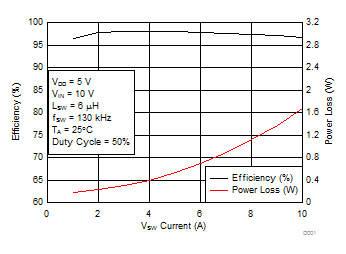
- 98% System Efficiency at 5 A
- Max Rated Continuous Current 10 A, Peak 15 A
- High-Frequency Operation (up to 600 kHz)
- High-Density SON 3.5 × 4.5 mm Footprint
- Ultra-Low Inductance Package
- System Optimized PCB Footprint
- 3.3-V and 5-V PWM Signal Compatible
- Input Voltages up to 24 V
- Integrated Bootstrap Diode
- Shoot-Through Protection
- RoHS Compliant – Lead Free Terminal Plating
- Halogen Free
- Optimized Power Stage Containing High-Efficiency Gate Drivers and FETs
- Optimized for 15-W Wireless Power Transmitter Designs
2 Applications
- WPC (Qi) 1.2 Compliant Wireless Power Transmitters for 15-W or 5-W Systems
- Proprietary Wireless Chargers and Transmitters
- Wirelessly Powered Industrial and Medical Systems
- For more information, see www.ti.com/wirelesspower
3 Description
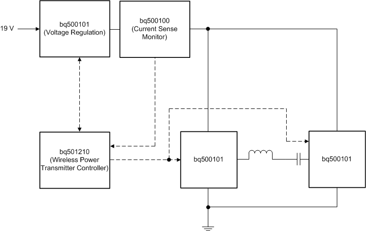
The bq500101 NexFET™ Power Stage is optimized for wireless power applications covering the WPC v1.2 medium power specification. The device can be used for both the rail voltage control in fixed frequency transmitter types as well as the coil drivers for both fixed and variable frequency types. This combination produces a high-current, high-efficiency, and high-speed switching device in a small 3.5 × 4.5 mm outline package. In addition, the PCB footprint is optimized to help reduce design time and simplify the completion of the overall system design.
Device Information(1)
| ORDER NUMBER | PACKAGE | BODY SIZE (NOM) | |
|---|---|---|---|
| bq500101 | DPC (9) | 3.5 mm x 4.5 mm | |
- For all available packages, see the orderable addendum at the end of the data sheet.
spacer
Application Diagram

Typical Power Stage Efficiency and Power Loss
