SNLS419D July 2012 – May 2015 DS125BR401
PRODUCTION DATA.
- 1 Features
- 2 Applications
- 3 Description
- 4 Typical Application
- 5 Revision History
- 6 Description (continued)
- 7 Pin Configuration and Functions
- 8 Specifications
- 9 Detailed Description
- 10Application and Implementation
- 11Power Supply Recommendations
- 12Layout
- 13Device and Documentation Support
- 14Mechanical, Packaging, and Orderable Information
1 Features
- Comprehensive Family, Proven System Interoperability
- DS125BR111: 1-Lane Repeater
- DS125BR401: 4-Lane Repeater
- DS125BR800: 8-Channel Repeater
- DS125MB203: 2-Port 2:1/1:2 Mux/Switch
- DS125DF410: 4-Channel Unidirectional Retimer With CDR
- Low 65-mW/Channel (Typical) Power Consumption, With Option to Power Down Unused Channels
- Nonlimiting Output for PCIe and 10G-KR Link Training Support
- Advanced Signal Conditioning Features
- Receive Equalization up to 30 dB at 6.25 GHz
- Transmit De-Emphasis up to –12 dB
- Transmit Output Voltage Control: 700 mV to 1300 mV
- Programmable Through Pin Selection, EEPROM, or SMBus Interface
- Single Supply Voltage: 2.5 V or 3.3 V (Selectable)
- −40°C to 85°C Operating Temperature Range
- 5-kV HBM ESD Rating
- Flow-Thru Pinout in 10-mm × 5.5-mm 54-Pin Leadless WQFN Package
- Supported Protocols
2 Applications
- SAS/SATA (up to 6 Gbps), Fibre Channel (up to 10 GFC)
- PCIe Gen-3/2/1, 10G-KR, 10GbE, XAUI, RXAUI
3 Description
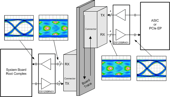
The DS125BR401 device is an extremely low-power high-performance multiprotocol repeater and redriver designed to support four lanes of PCIe Gen-3/2/1, 10G-KR, and other high-speed interface serial protocols up to 12.5 Gbps. The continuous time linear equalizer (CTLE) of the receiver provides a boost of up to 30 dB at 6.25 GHz (12.5 Gbps) in each of its eight channels and can open an input eye that is completely closed due to intersymbol interference (ISI) induced by interconnect medium such as backplane traces of 30 inches or more or copper cables of 8 meters or more, hence enabling host controllers to ensure an error-free end-to-end link. The transmitter provides a de-emphasis boost of up to –12 dB and output voltage amplitude control from 700 mV to 1300 mV to allow maximum flexibility in the physical placement within the interconnect channel.
Device Information(1)
| PART NUMBER | PACKAGE | BODY SIZE (NOM) |
|---|---|---|
| DS125BR401 | WQFN (54) | 10.00 mm × 5.50 mm |
- For all available packages, see the orderable addendum at the end of the data sheet.
4 Typical Application
