SBOA326 May 2021 OPA197 , OPA2991
Design Goals
| Input | Output | Supply | |||||
|---|---|---|---|---|---|---|---|
| ViMin | ViMax | IiMax | IoMin | IoMax | PR5Max | Vcc | Vee |
| 0V | 10V | 200µA | 0A | 5A | 0.25W | 36V | 0V |
Design Description
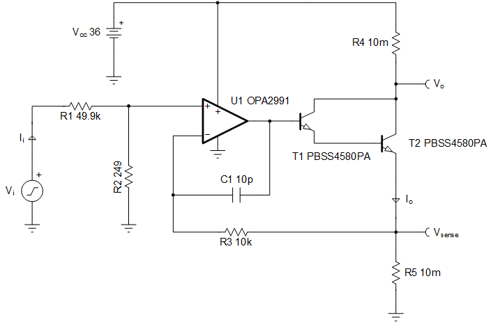
This high-side voltage-to-current (V-I) converter delivers a well-regulated current to a load, R4. The circuit accepts an input voltage from 0V to 10V and converts it to an output current from 0A to 5A. The current is regulated by feeding the voltage across a low-side, current-sense resistor back to the op amp. The output Darlington pair allows for higher current gain than when using a single, discrete transistor.
Design Notes
- A resistor divider, formed by R1 and R2, is implemented at the input to limit the full-scale voltage at the non-inverting terminal of the amplifier and the output sense resistor (R5).
- The high current gain of the Darlington pair reduces the demand on the output current of the op amp.
- Smaller values of R4 and R5 lead to an increased load compliance voltage and a reduction in power dissipated in the full-scale, output state.
- Feedback components R3 and C1 provide frequency compensation to ensure the stability of the circuit during transients. They also help reduce noise. R3 provides a DC feedback path directly at the current setting resistor, R5, and C1 provides a high-frequency feedback path that bypasses the NPN pair.
- The input bias current will flow through R3, which will cause a DC error. Therefore, ensure that this error is minimal compared to the offset voltage of the op amp.
- Select an op amp whose linear output voltage swing includes at least 2 ✕ Vbe+Vsense. The output voltage of the op amp will be greater than the voltage at the sense resistor by approximaly double the base-to-emitter voltage, Vbe.
- Use the op amp in its linear operating region, specified under the AOL test conditions of the data sheet.
- If needed, an isolation resistor may be placed between the high-frequency feedback path and the base of T1 for stability.
Design Steps
The transfer function of this circuit is provided in the following steps:
- Using the specifications for the maximum output power dissipation and the maximum output current, determine the maximum value of Vsense.
- Calculate the sense resistance, R5.
- Select values for R1 and R2 based on the maximum allowable input current, IiMax, and the desired VsenseMax voltage.
- See the Design References section [2] for the design procedure on how to properly size the compensation components, R3 and C1.
Design Simulations
DC Simulation Results
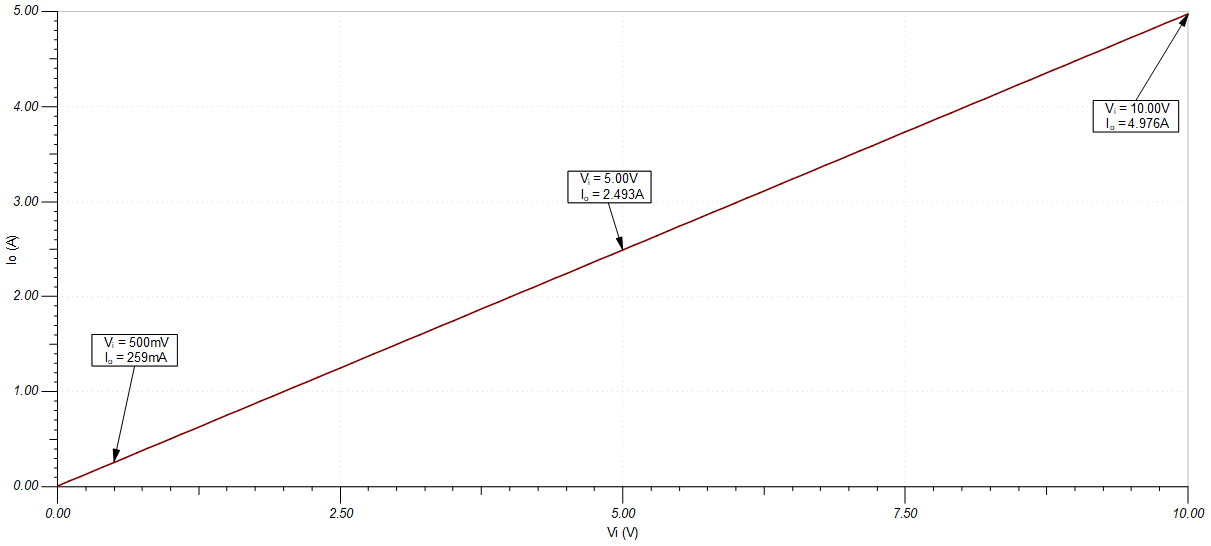
Loop Stability Simulation Results
Loop gain phase is 53 degrees.
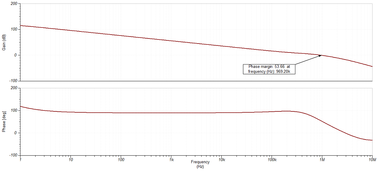
Compliance Voltage Simulation Results
Design References
- See Analog Engineer's Circuit Cookbooks for TI's comprehensive circuit library.
- TI Precision Labs
Design Featured Op Amp
| OPA2991 | |
|---|---|
| Vss | 2.7V to 40V |
| VinCM | Rail-to-rail |
| Vout | Rail-to-rail |
| Vos | 125µV |
| Iq | 560µA |
| Ib | 10pA |
| UGBW | 4.5MHz |
| SR | 21V/µs |
| #Channels | 1, 2, 4 |
| www.ti.com/product/opa2991 | |
Design Alternate Op Amp
| OPA197 | |
|---|---|
| Vss | 4.5V to 36V |
| VinCM | Rail-to-rail |
| Vout | Rail-to-rail |
| Vos | 25µV |
| Iq | 1mA |
| Ib | 5pA |
| UGBW | 10MHz |
| SR | 20V/µs |
| #Channels | 1, 2, 4 |
| www.ti.com/product/opa197 | |