SLAA985 December 2020 MSP430FR2433
1 TI Tech Note
Introduction
Many applications require simple I/Os functions such as blinking multiple LEDs; however, there may be not enough general-purpose I/O pins for the host microcontroller (MCU) or processor to perform these tasks. The synchronous peripheral interface (SPI) enables serial communication between the MSP430™ microcontroller and host, which can be acting as an I/O expander with SPI communication. The MSP430FR2433 MCU can be a SPI peripheral device using the enhanced Serial Communication Interface (eUSCI) module to receive commands from the host and control the 8 general-purpose I/O pins.
The following functions can be expanded:
- SPI interface to expand with 8 simple I/O pins
- Set I/O output value (port, group, or bit)
- Read I/O input value (port, group, or bit)
Implementation
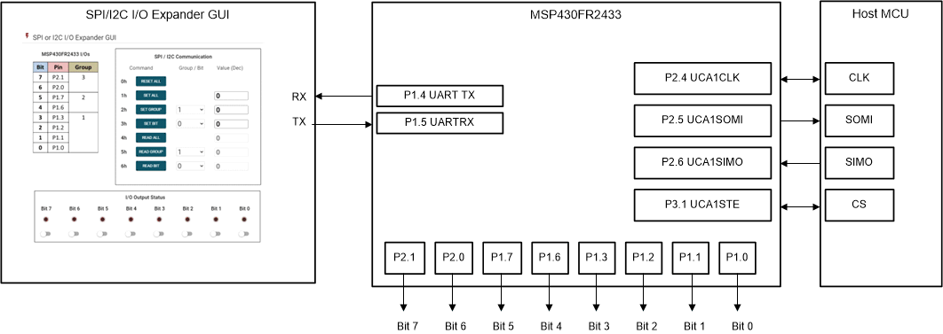
A host processor acting as the controller should be connected so it can write or read data from the eUSCI_A0 of MSP430FR2433 MCU through the 4-wire SPI bus [SPI clock (SCLK), MOSI, MISO, and CS/STE]. There are 8 pins being expanded from the SPI commands. Figure 1-1 shows the SPI I/O Expander block diagram interface.
 Figure 1-1 SPI I/O Expander Block
Diagram
Figure 1-1 SPI I/O Expander Block
DiagramThe host processor SPI configuration is as follows:
- 4-pin SPI with STE/CS active low
- Clock polarity inactive state high
- Data is changed on the first UCLK edge and captured on the following edge
- Most significant bit (MSB) first, 8-bit character length
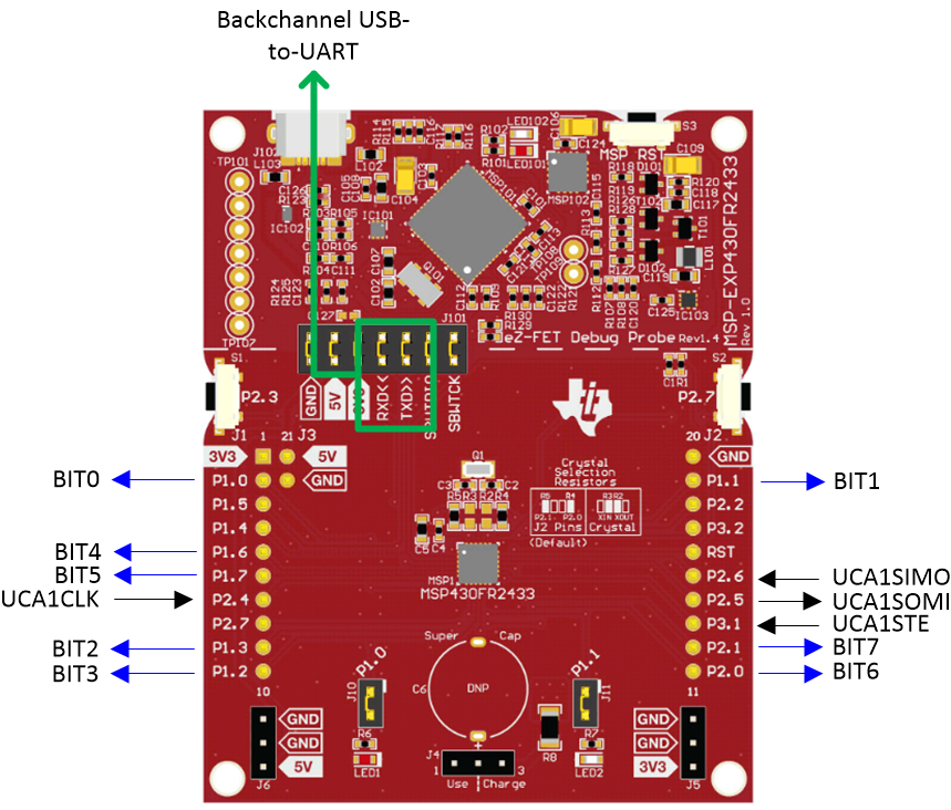
The STE pin determines if the SPI is enabled and is active low by default. Communication is achieved by sending a 24-bit message, in which the first byte is the command, the second byte selects the group or bit number, and the third is the data. Then the MSP430FR2433 device outputs the data to or reads the data from the mapped I/O pins defined in the software. The pinout and connections on the MSP430FR2433 LaunchPad development board are shown in Figure 1-2.
 Figure 1-2 MSP430FR2433 LaunchPad
Connections
Figure 1-2 MSP430FR2433 LaunchPad
ConnectionsThe 24-bit message sent out by the host is transmitted with three bytes of data on the SPI interface. The first byte is the Host Command, which tells the peripheral device what operation should be done for the pins. Command options are Reset All (0h), Set All (1h), Set Group (2h), Set Bit (3h), Read All (4h), Read Group (5h), and Read Bit (6h). Table 1-1 lists the 8-bit Host Command values.
| Host Command | Value (Hex) |
|---|---|
| Reset All | 0x00 |
| Set All | 0x01 |
| Set Group | 0x02 |
| Set Bit | 0x03 |
| Read All | 0x04 |
| Read Group | 0x05 |
| Read Bit | 0x06 |
The 8-bit Data Index value determines which group or bit number to write data to when using a Set Group, Set Bit, Read Group, or Read Bit command. The 8-bit I/O port defined for the MSP430FR2433 example code divides the port into 3 groups: Group 1 (Bits 3-0), Group 2 (Bits 5-4), and Group 3 (Bits 7-6). If selecting a Reset All, Set All, or Read All command, then this byte is a “Don’t Care”. Table 1-2 lists the 8-bit Data Index values.
| Data Index / Select | Value (Hex) |
|---|---|
| Bit 0 | 0x00 |
| Bit 1 / Group 1 | 0x01 |
| Bit 2 / Group 2 | 0x02 |
| Bit 3 / Group 3 | 0x03 |
| Bit 4 | 0x04 |
| Bit 5 | 0x05 |
| Bit 6 | 0x06 |
| Bit 7 | 0x07 |
| All | Don't Care |
Data Value (see Table 1-3 ) tells the value to be outputted to the I/O port, specified group, or specified bit. For a Set command (1h, 2h, or 3h), the data D7-D0 represents the 8-bit value to be sent to the selected output. For the Reset All command or any Read command, the 8-bit data is a “Don’t Care”. Table 1-3 lists the 8-bit data values.
| D7 | D6 | D5 | D4 | D3 | D2 | D1 | D0 | |
|---|---|---|---|---|---|---|---|---|
| Reset All | X | X | X | X | X | X | X | X |
| Set All | D7 | D6 | D5 | D4 | D3 | D2 | D1 | D0 |
| Set Group | X | X | X | X | D3 | D2 | D1 | D0 |
| Set Bit | X | X | X | X | X | X | X | D0 |
| Read All | X | X | X | X | X | X | X | X |
| Read Group | X | X | X | X | X | X | X | X |
| Read Bit | X | X | X | X | X | X | X | X |
Performance
The host processor sends the host command and data to the MSP430FR2433 MCU using a specified bit rate. The bit rate in the SPI I/O Expander code example is approximately 1 MHz. The time between the STE start of host command and the STE stop of data depends on the SPI configuration of host processor.
The time for action of MSP430FR2433 MCU depends on the CPU clock frequency and the low-power mode (LPM) setting of the device. The following test results used the default 1-MHz CPU clock frequency and LPM0 for standby. The action time can be optimized by using a higher CPU clock frequency, which may increase code size to configure the CPU clock, as well as a lower low-power mode to let the CPU wake up from LPM mode more quickly.
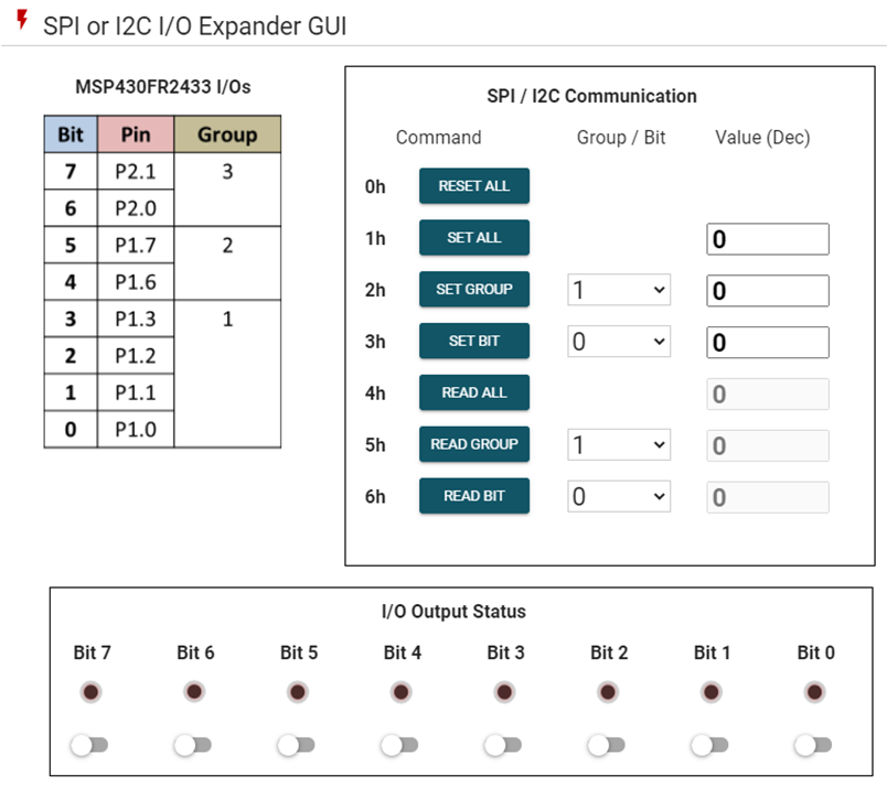
 Figure 1-3 SPI I/O Expander GUI
As shown in Figure 1-3, a GUI is used to 1) monitor the initiated SPI transactions and update the status of the MSP430FR2433 I/O pins with a virtual LED array or 2) act as the host application to expand the I/O pins over backchannel USB-to-UART.
When using the GUI as a monitor, it will update the data values to the associated command and group/bit value initiated over the 3-byte SPI transaction. Furthermore, if a Set command is issued, it will update the virtual LED array with the values specified from the data byte of the transaction. For instance, if a 3-byte SPI transaction is 0x03, 0x02, 0x01, then a “Set Bit” command is issued, Bit 2 is the specified bit, and it will write a value of “1”. P1.2 will go high, the GUI will update the “Group/Bit” value to “2”, and the “Data” value will update to “1” for the “Set Bit” row. Additionally, the LED and switch for Bit 2 will go into the “ON” state.
Alternatively, the GUI can serve as the host application using backchannel USB-to-UART. The user can click on a Command button to initiate a Reset All, Set, or Read command for all, a group, or a bit. Ensure the “Group/Bit” and/or “Data” values are set before initiating a command. Additionally, switches are available below the LEDs to individually set or clear bits. To initiate the same command as before, update the “Group/Bit” value to “2” and the “Data” value to “1”, then click on the “Set Bit” command to initiate the command. P1.2 will go high and the Bit 2 LED and switch will go into the “ON” state.
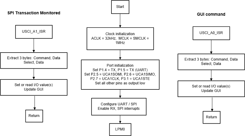
A code flowchart is provided in Figure 1-4 to simplify understanding of the software. A SPI transaction or GUI command triggers an interrupt to set or read the I/O values and update the GUI.
 Figure 1-4 Software Flowchart
To Get Started
- Watch the training video “SPI I/O Expander”, showing a walk through on how to use Serial Peripheral Interface to expand SPI data from a host MCU into the secondary’s I/O ports.
- Order a MSP430FR2433 LaunchPad kit to evaluate the SPI I/O Expander example Code.
- Download and test this example with the SPI I/O Expander example GUI.
- Evaluate the SPI I/O Expander example code for the MSP430FR2433 LaunchPad kit.
Device Recommendations
| Part Number | Key Features |
|---|---|
| MSP430FR2433 | 16KB FRAM, 4KB SRAM, 10-bit ADC, UART/SPI/I2C, Timer |
| MSP430FR2422 | 8KB FRAM, 2KB SRAM, 10-bit ADC, UART/SPI/I2C, Timer |