SLLA190A March 2006 – March 2022 INA138 , INA138-Q1 , INA139 , INA139-Q1 , INA168 , INA168-Q1 , INA169 , INA169-Q1
1
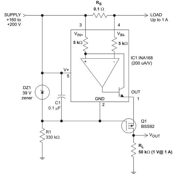
Many current shunt monitor integrated circuits (IC) support a common-mode voltage maximum rating ranging from 26 V to 120 V. However, sometimes it is necessary to have a common-mode voltage that is higher than the specified maximum of the device. The circuit in Figure 1-1 shows one method of how current shunt monitor ICs, such as the Texas Instruments INA168, can be used with even higher common-mode voltages than specified in the data sheet. This method can be extended to any voltage as long as a suitable MOSFET (Q1) can be found. The rest of this application brief describes the function of the needed components as well as key design parameters used to create the circuit shown in Figure 1-1.
 Figure 1-1 Example Circuit That
Extends the Common-Mode Voltage Range of the
INA168
Figure 1-1 Example Circuit That
Extends the Common-Mode Voltage Range of the
INA168Zener diode DZ1 regulates the supply voltage that the current shunt monitor operates within, and this voltage floats relative to the supply voltage. DZ1 is chosen to provide sufficient operating voltage for the combination of IC1 and Q1 over the expected power-supply range (typically from 5.1 V to 56 V). Select R1 to set the bias current for DZ1 at some value greater than the maximum quiescent current of IC1. The INA168 shown in Figure 1-1 is specified at 45 µA maximum. The bias current in DZ1 is approximately 500 μA at 200 V, well in excess of the maximum current of IC1 (the bias current value was selected to limit dissipation in R1 to less than 0.1 W).
Connect a P-channel MOSFET, Q1, as shown to cascode the output current of IC1 down to or below ground level. The voltage rating of transistor Q1 should exceed the difference between the total supply and DZ1 by several volts because of the upward voltage swing on the source of Q1. Select RL, the load resistor of IC1, as if IC1 were used alone.
The cascode connection of Q1 enables using IC1 well in excess of its normal 60-V rating. The example circuit shown in Figure 1-1 was specifically designed to operate from 160 V to 200 V, and sense up to 1 A of current at a 1-V full-scale output.
| Document Number | Document Title | Relevancy |
|---|---|---|
| SBOA358 | Adjustable-gain, current-output, high-side current-sensing circuit | A circuit design that can be used to convert a voltage-output device into a current-output circuit so that it can be used with the circuit shown in Figure 1-1. |
| TIDA-00332 | High Voltage 12 V – 400 V DC Current Sense Reference Design | A Reference Design using a similar circuit to the one shown in Figure 1-1, but with the INA138. |
| TIDA-00313 | –48-V Telecom Current/Voltage/Power Sense with Isolation | A Reference Design showing how to use any common-mode voltage with a floating power supply and isolation for digital devices. |
| SBOA198 | Extending Beyond the Max Common-Mode Range of Discrete Current-Sense Amplifiers | An Application Brief covering different methods of extending the common-mode voltage range, including the example used in Figure 1-1. |