SNAS407H August 2007 – April 2015
PRODUCTION DATA.
- 1 Features
- 2 Applications
- 3 Description
- 4 Revision History
- 5 Description (continued)
- 6 Pin Configuration and Functions
- 7 Specifications
- 8 Detailed Description
- 9 Application and Implementation
- 10Power Supply Recommendations
- 11Layout
- 12Device and Documentation Support
- 13Mechanical, Packaging, and Orderable Information
1 Features
- Ensured Monotonicity
- Low Power Operation
- Rail-to-Rail Voltage Output
- Daisy-Chain Capability
- Power-on Reset to 0 V
- Simultaneous Output Updating
- Individual Channel Power-Down Capability
- Wide Power Supply Range (2.7 V to 5.5 V)
- Dual Reference Voltages With Range of 0.5 V to VA
- Operating Temperature Range of −40°C to 125°C
- Smallest Package in the Industry
- Resolution 12 Bits
- INL ±8 LSB (Maximum)
- DNL 0.75 / −0.4 LSB (Maximum)
- Settling Time 8.5 μs (Maximum)
- Zero Code Error 15 mV (Maximum)
- Full-Scale Error −0.75 %FSR (Maximum)
- Supply Power
- 1.95 mW (3 V) / 4.85 mW (5 V) Typical
- Power Down 0.3 μW (3 V) / 1 μW (5 V) Typical
2 Applications
- Battery-Powered Instruments
- Digital Gain and Offset Adjustment
- Programmable Voltage and Current Sources
- Programmable Attenuators
- Voltage Reference for ADCs
- Sensor Supply Voltage
- Range Detectors
3 Description
The DAC128S085 is a full-featured, general-purpose OCTAL 12-bit voltage-output digital-to-analog converter (DAC) that can operate from a single 2.7-V to 5.5-V supply and consumes 1.95 mW at 3 V and 4.85 mW at 5 V. The DAC128S085 is packaged in a 16-lead WQFN package and a 16-lead TSSOP package. The WQFN package makes the DAC128S085 the smallest OCTAL DAC in its class. The on-chip output amplifiers allow rail-to-rail output swing, and the 3-wire serial interface operates at clock rates up to 40 MHz over the entire supply voltage range. Competitive devices are limited to 25-MHz clock rates at supply voltages in the 2.7-V to 3.6-V range. The serial interface is compatible with standard SPI™, QSPI, MICROWIRE, and DSP interfaces. The DAC128S085 also offers daisy-chain operation, where an unlimited number of DAC128S085s can be updated simultaneously using a single serial interface.
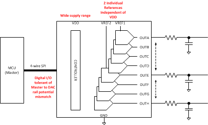
There are two references for the DAC128S085. One reference input serves channels A through D, while the other reference serves channels E through H. Each reference can be set independently between 0.5 V and VA, providing the widest possible output dynamic range. The DAC128S085 has a 16-bit input shift register that controls the mode of operation, the power-down condition, and the register/output value of the DAC channels. All eight DAC outputs can be updated simultaneously or individually.
Device Information(1)
| PART NUMBER | PACKAGE | BODY SIZE (NOM) |
|---|---|---|
| DAC128S085 | TSSOP (16) | 5.00 mm × 4.4 mm |
| WQFN (16) | 4.00 mm × 4.00 mm |
- For all available packages, see the orderable addendum at the end of the datasheet.
Simplified Schematic
