SLLSE57E April 2011 – March 2015 SN75DP130
PRODUCTION DATA.
- 1 Features
- 2 Applications
- 3 Description
- 4 Revision History
- 5 Description (continued)
- 6 Pin Configuration and Functions
- 7 Specifications
- 8 Parameter Measurement Information
- 9 Detailed Description
- 10Application and Implementation
- 11Power Supply Recommendations
- 12Layout
- 13Device and Documentation Support
- 14Mechanical, Packaging, and Orderable Information
パッケージ・オプション
メカニカル・データ(パッケージ|ピン)
- RGZ|48
サーマルパッド・メカニカル・データ
- RGZ|48
発注情報
1 Features
- Supports DP v1.1a and DP v1.2 Signaling Including HBR2 Data Rates to 5.4 Gbps
- Supports HDMI 1.4b With TMDS Clock Frequencies up to 340 MHz
- Glueless Interface to AMD, Intel, and NVIDIA Graphics Processors
- Auto-Configuration Through Link Training
- Output Signal Conditioning With Tunable Voltage Swing and Pre-Emphasis Gain
- Highly Configurable Input Variable Equalizer
- Two Device Options Including a Dual Power Supply Configuration for Lowest Power
- 2-kV ESD HBM Protection
- Temperature Range: 0°C to 85°C
- 48-Pin 7-mm × 7-mm VQFN Package
2 Applications
- Notebook PCs
- Desktop PCs
- PC Docking Stations
- PC Standalone Video Cards
3 Description
The SN75DP130 device is a single channel DisplayPort™ (DP) re-driver that regenerates the DP high-speed digital link. The device complies with the VESA DisplayPort Standard Version 1.2, and supports a 4-lane Main Link interface signaling up to HBR2 rates at 5.4 Gbps per lane. This device also supports DP++ Dual-Mode, offering TMDS signaling for DVI and full HDMI Version 1.4a support.
The device compensates for PCB-related frequency loss and switching-related loss to provide the optimum DP electrical performance from source to sink. The Main Link signal inputs feature configurable equalizers with selectable boost settings. At the Main Link output, four primary levels of differential output voltage swing (VOD) and four primary levels of pre-emphasis are available. A secondary level of boost adjustment, programmed through I2C, for fine-tuning the Main Link output. The device can monitor the AUX channel and automatically adjust the output signaling levels and input equalizers in response to Link Training commands. Additionally, the SN75DP130 output signal conditioning and EQ parameters are fully programmable through the I2C interface.
Device Information(1)
| PART NUMBER | PACKAGE | BODY SIZE (NOM) |
|---|---|---|
| SN75DP130 | VQFN (48) | 7.00 mm × 7.00 mm |
- For all available packages, see the orderable addendum at the end of the data sheet.
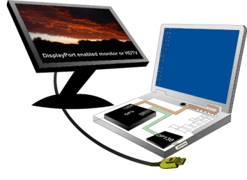
Simple Application
