SLUSBW8 September 2014 TPS53632
PRODUCTION DATA.
- 1 Features
- 2 Applications
- 3 Description
- 4 Revision History
- 5 Pin Configuration and Functions
- 6 Specifications
-
7 Detailed Description
- 7.1 Overview
- 7.2 Functional Block Diagram
- 7.3
Feature Description
- 7.3.1 Current Sensing
- 7.3.2 Load Transients
- 7.3.3 AutoBalance Current Sharing
- 7.3.4 PWM and SKIP Signals
- 7.3.5 5-V, 3.3-V and 1.8-V Undervoltage Lockout (UVLO)
- 7.3.6 Output Undervoltage Protection (UVP)
- 7.3.7 Overcurrent Protection (OCP)
- 7.3.8 Overvoltage Protection
- 7.3.9 Analog Current Monitor, IMON and Corresponding Digital Output Current
- 7.3.10 Addressing
- 7.3.11 I2C Interface Operation
- 7.3.12 Start-Up Sequence
- 7.3.13 Phase Add and Drop Operation
- 7.3.14 Power Good Operation
- 7.3.15 Input Voltage Limits
- 7.3.16 Fault Behavior
- 7.4 Device Functional Modes
- 7.5 Configuration and Programming
- 7.6 Register Maps
-
8 Applications and Implementation
- 8.1
Application Information
- 8.1.1
3-Phase D-CAP+™, Step-Down Application
- 8.1.1.1 Design Requirements
- 8.1.1.2
Detailed Design Procedure
- 8.1.1.2.1 Step 1: Select Switching Frequency
- 8.1.1.2.2 Step 2: Set The Slew Rate
- 8.1.1.2.3 Step 3: Determine Inductor Value And Choose Inductor
- 8.1.1.2.4 Step 4: Determine Current Sensing Method
- 8.1.1.2.5 Step 5: DCR Current Sensing
- 8.1.1.2.6 Step 6: Select OCP Level
- 8.1.1.2.7 Step 7: Set the Load-Line Slope
- 8.1.1.2.8 Step 8: Current Monitor (IMON) Setting
- 8.1.1.3 Application Performance Plots
- 8.1.1.4 Loop Compensation for Zero Load-Line
- 8.1.1
3-Phase D-CAP+™, Step-Down Application
- 8.1
Application Information
- 9 Power Supply Recommendations
- 10 Layout
- 11Device and Documentation Support
- 12Mechanical, Packaging, and Orderable Information
1 Features
- Selectable Phase Count: (3, 2, or 1)
- I2C Interface for VID Control and Telemetry with Eight Device Addresses
- D-CAP+™ Control for Fast Transient Response
- Dynamic Phase Add and Drop Operation
- Switching Frequency: 300 kHz to 1 MHz
- Digital Current Monitor
- 7-Bit, DAC Output Range: 0.50 V to 1.52 V
- Optimized Efficiency at Light and Heavy Loads
- Accurate, Adjustable Voltage Positioning or Zero Slope Load-Line
- Patented AutoBalance™ Phase Balancing
- Selectable, 8-Level Current Limit
- 2.5-V to 24-V Conversion Voltage Range
- Default Boot Voltage: 1.00 V
- Small, 4-mm x 4-mm, 32-Pin, VQFN PowerPAD Package
2 Applications
- High-Current, Low-Voltage Applications
- Core Power for Microservers, Custom Microcontrollers, ASICs
3 Description
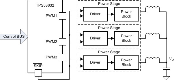
The TPS53632 device is a driverless step-down controller with serial control. Advanced features such as D-CAP+ architecture provide fast transient response, lowest output capacitance and high efficiency. The TPS53632 device supports the standard I2C Rev 3.0 interface for dynamic control of the output voltage and current monitor telemetry. It also has dynamic phase add and drop control and enters single-phase, discontinuous-current-mode operation to maximize light-load efficiency.
Other features include adjustable control of VCORE slew rate and voltage positioning. The TPS51604 device driver is designed specifically for this generation of controllers. In addition, the TPS53632 device can be used along with the TI power stage devices (driver MOSFETs). The TPS53632 device is packaged in a space saving, thermally enhanced, 32-pin VQFN package and is rated to operate at a range between –10°C and 105°C.
Device Information
| PART NUMBER | PACKAGE | BODY SIZE |
|---|---|---|
| TPS53632 | VQFN | 4 mm × 4 mm |
Simplified Schematic