SNVSA76B March 2015 – March 2017 TPS61177A
PRODUCTION DATA.
- 1 Features
- 2 Applications
- 3 Description
- 4 Revision History
- 5 Pin Configuration and Functions
- 6 Specifications
-
7 Detailed Description
- 7.1 Overview
- 7.2 Functional Block Diagram
- 7.3
Feature Description
- 7.3.1 Supply Voltage
- 7.3.2 Boost Regulator
- 7.3.3 Programmable Switch Frequency and Slew Rate
- 7.3.4 LED Current Sinks
- 7.3.5 Enable and Start-Up Timing
- 7.3.6 Input Undervoltage Protection (UVLO)
- 7.3.7 Overvoltage Protection (OVP)
- 7.3.8 Current-Sink Open Protection
- 7.3.9 Overcurrent Protection
- 7.3.10 Thermal Protection
- 7.4 Device Functional Modes
- 7.5 Programming
- 7.6
Register Maps
- 7.6.1 MODE (A0h)
- 7.6.2 CS (A1h)
- 7.6.3 UVLO (A2h)
- 7.6.4 FREQ (A3h)
- 7.6.5 SR (A4h)
- 7.6.6 ILIM (A5h)
- 7.6.7 Control (FFh)
- 7.6.8 Example - Writing to a Single RAM Register
- 7.6.9 Example - Writing to Multiple RAM Registers
- 7.6.10 Example - Saving Contents of all RAM Registers to E2PROM
- 7.6.11 Example - Reading from a Single RAM Register
- 7.6.12 Example - Reading from a Single E2PROM Register
- 7.6.13 Example - Reading from Multiple RAM Registers
- 7.6.14 Example - Reading from Multiple E2PROM Registers
- 8 Application and Implementation
- 9 Power Supply Recommendations
- 10Layout
- 11Device and Documentation Support
- 12Mechanical, Packaging, and Orderable Information
パッケージ・オプション
メカニカル・データ(パッケージ|ピン)
- RGR|20
サーマルパッド・メカニカル・データ
- RGR|20
発注情報
1 Features
- 2.5-V to 24-V Input Voltage Range
- 39-V Maximum Output Voltage
- Integrated 1.8-A, 40-V MOSFET
- 450-kHz to 1.2-MHz Programmable Switching Frequency
- Adaptive Boost Output to WLED Voltages
- 100-Hz to 25-kHz Wide Input PWM Dimming Frequency Range
- 1% Minimum Dimming Duty Cycle
- Small External Components
- Integrated Loop Compensation
- Six Current Sinks of 30 mA Maximum
- 1% (Typical) Current Matching
- Input PWM Glitch Filter
- PWM Brightness Interface Control
- Three Optional Dimming Methods, including Direct PWM Dimming, Analog Dimming, and Analog and PWM Mixed Dimming
- Built-in WLED Open Protection
- Thermal Shutdown
2 Applications
- Notebook and Tablet LCD Display Backlights
- Patient Monitors
- Medical Displays
- HMI
- Test and Measurement Equipment
3 Description
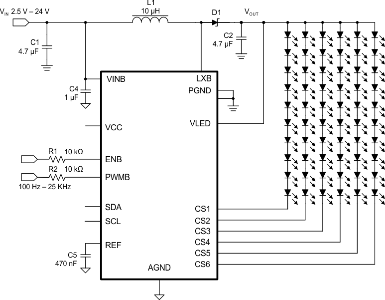
The TPS61177A device provides a highly integrated white LED (WLED) driver solution for notebook LCD backlight. This device has a built-in high-efficiency boost regulator with integrated 1.8-A, 40-V power MOSFET. The six current sink regulators provide high precision current regulation and matching. In total, the device can support up to 72 WLEDs. In addition, the boost output automatically adjusts its voltage to the WLED forward voltage to optimize efficiency.
The TPS61177A supports the analog dimming, analog and PWM dimming, and direct PWM dimming method. During analog dimming mode, each CS current linearly varies depending on the duty cycle information on the PWMB pin. During analog and PWM mixed dimming mode, the input PWM duty cycle information is translated to an analog signal to control the WLED current linearly over 25% to 100% brightness area. The device also allows adding PWM dimming when the analog current is down to 25%. Below 25%, the analog signal translates to PWM duty cycle information to control the on or off of WLED current and averages the WLED current down to 1%. The frequency of adding PWM dimming is same to input PWM frequency on the PWMB pin. While the TPS61177A also supports a direct PWM dimming method, in direct PWM dimming mode the WLED current is turned on or off, synchronized with the input PWM signal.
Device Information(1)
| PART NUMBER | PACKAGE | BODY SIZE (NOM) |
|---|---|---|
| TPS61177A | VQFN (20) | 3.50 mm x 3.50 mm |
- For all available packages, see the orderable addendum at the end of the data sheet.
Typical Application – Analog and PWM Mixed Mode
