SLUS822C June 2008 – August 2016 UCC27200-Q1
PRODUCTION DATA.
- 1 Features
- 2 Applications
- 3 Description
- 4 Revision History
- 5 Pin Configuration and Functions
- 6 Specifications
- 7 Detailed Description
- 8 Application and Implementation
- 9 Power Supply Recommendations
- 10Layout
- 11Device and Documentation Support
- 12Mechanical, Packaging, and Orderable Information
パッケージ・オプション
メカニカル・データ(パッケージ|ピン)
- DDA|8
サーマルパッド・メカニカル・データ
- DDA|8
発注情報
1 Features
- Qualified for Automotive Applications
- AEC-Q100 Qualified With the Following Results:
- Drives Two N-Channel MOSFETs in High-Side and Low-Side Configuration
- Maximum Boot Voltage: 120 V
- Maximum VDD Voltage: 20 V
- On-Chip 0.65-V VF, 0.6-Ω RD Bootstrap Diode
- Greater than 1 MHz of Operation
- 20-ns Propagation Delay Times
- 3-A Sink, 3-A Source Output Currents
- 8-ns Rise and 7-ns Fall Time With 1000-pF Load
- 1-ns Delay Matching
- Specified from –40°C to 140°C (Junction Temperature)
2 Applications
- Power Supplies for Telecom, Datacom, and Merchant Markets
- Half-Bridge Applications and Full-Bridge Converters
- Isolated Bus Architecture
- Two-Switch Forward Converters
- Active-Clamp Forward Converters
- High-Voltage Synchronous-Buck Converters
- Class-D Audio Amplifiers
3 Description
The UCC2720x-Q1 family of high-frequency N-channel MOSFET drivers include a 120-V bootstrap diode and high-side and low-side drivers with independent inputs for maximum control flexibility. This allows for N-channel MOSFET control in half-bridge, full-bridge, two-switch forward, and active-clamp forward converters. The low-side and the high-side gate drivers are independently controlled and matched to 1 ns between the turnon and turnoff of each other.
An on-chip bootstrap diode eliminates the external discrete diodes. Undervoltage lockout is provided for both the high-side and the low-side drivers, forcing the outputs low if the drive voltage is below the specified threshold.
Two versions of the UCC2720x-Q1 are offered – the UCC27200-Q1 has high-noise-immune CMOS input thresholds, and the UCC27201-Q1 has TTL-compatible thresholds.
Both devices are offered in the 8-pin SO PowerPAD™ (DDA) package.
Device Information(1)
| PART NUMBER | PACKAGE | BODY SIZE (NOM) |
|---|---|---|
| UCC2720x-Q1 | SO PowerPAD (8) | 4.89 mm × 3.90 mm |
- For all available packages, see the orderable addendum at the end of the data sheet.
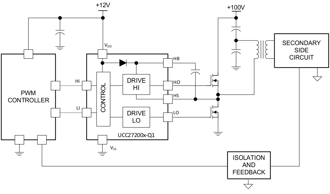
Simplified Application Diagram
