JAJS373D May   2009  – January 2018 ADS1113 , ADS1114 , ADS1115

PRODUCTION DATA.  

  1. 特長
  2. アプリケーション
  3. 概要
    1.     Device Images
      1.      概略ブロック図
  4. 改訂履歴
  5. Device Comparison Table
  6. Pin Configuration and Functions
    1.     Pin Functions
  7. Specifications
    1. 7.1 Absolute Maximum Ratings
    2. 7.2 ESD Ratings
    3. 7.3 Recommended Operating Conditions
    4. 7.4 Thermal Information
    5. 7.5 Electrical Characteristics
    6. 7.6 Timing Requirements: I2C
    7. 7.7 Typical Characteristics
  8. Parameter Measurement Information
    1. 8.1 Noise Performance
  9. Detailed Description
    1. 9.1 Overview
    2. 9.2 Functional Block Diagrams
    3. 9.3 Feature Description
      1. 9.3.1 Multiplexer
      2. 9.3.2 Analog Inputs
      3. 9.3.3 Full-Scale Range (FSR) and LSB Size
      4. 9.3.4 Voltage Reference
      5. 9.3.5 Oscillator
      6. 9.3.6 Output Data Rate and Conversion Time
      7. 9.3.7 Digital Comparator (ADS1114 and ADS1115 Only)
      8. 9.3.8 Conversion Ready Pin (ADS1114 and ADS1115 Only)
      9. 9.3.9 SMbus Alert Response
    4. 9.4 Device Functional Modes
      1. 9.4.1 Reset and Power-Up
      2. 9.4.2 Operating Modes
        1. 9.4.2.1 Single-Shot Mode
        2. 9.4.2.2 Continuous-Conversion Mode
      3. 9.4.3 Duty Cycling For Low Power
    5. 9.5 Programming
      1. 9.5.1 I2C Interface
        1. 9.5.1.1 I2C Address Selection
        2. 9.5.1.2 I2C General Call
        3. 9.5.1.3 I2C Speed Modes
      2. 9.5.2 Slave Mode Operations
        1. 9.5.2.1 Receive Mode
        2. 9.5.2.2 Transmit Mode
      3. 9.5.3 Writing To and Reading From the Registers
      4. 9.5.4 Data Format
    6. 9.6 Register Map
      1. 9.6.1 Address Pointer Register (address = N/A) [reset = N/A]
        1. Table 6. Address Pointer Register Field Descriptions
      2. 9.6.2 Conversion Register (P[1:0] = 0h) [reset = 0000h]
        1. Table 7. Conversion Register Field Descriptions
      3. 9.6.3 Config Register (P[1:0] = 1h) [reset = 8583h]
        1. Table 8. Config Register Field Descriptions
      4. 9.6.4 Lo_thresh (P[1:0] = 2h) [reset = 8000h] and Hi_thresh (P[1:0] = 3h) [reset = 7FFFh] Registers
        1. Table 9. Lo_thresh and Hi_thresh Register Field Descriptions
  10. 10Application and Implementation
    1. 10.1 Application Information
      1. 10.1.1 Basic Connections
      2. 10.1.2 Single-Ended Inputs
      3. 10.1.3 Input Protection
      4. 10.1.4 Unused Inputs and Outputs
      5. 10.1.5 Analog Input Filtering
      6. 10.1.6 Connecting Multiple Devices
      7. 10.1.7 Quickstart Guide
    2. 10.2 Typical Application
      1. 10.2.1 Design Requirements
      2. 10.2.2 Detailed Design Procedure
        1. 10.2.2.1 Shunt Resistor Considerations
        2. 10.2.2.2 Operational Amplifier Considerations
        3. 10.2.2.3 ADC Input Common-Mode Considerations
        4. 10.2.2.4 Resistor (R1, R2, R3, R4) Considerations
        5. 10.2.2.5 Noise and Input Impedance Considerations
        6. 10.2.2.6 First-order RC Filter Considerations
        7. 10.2.2.7 Circuit Implementation
        8. 10.2.2.8 Results Summary
      3. 10.2.3 Application Curves
  11. 11Power Supply Recommendations
    1. 11.1 Power-Supply Sequencing
    2. 11.2 Power-Supply Decoupling
  12. 12Layout
    1. 12.1 Layout Guidelines
    2. 12.2 Layout Example
  13. 13デバイスおよびドキュメントのサポート
    1. 13.1 ドキュメントのサポート
      1. 13.1.1 関連資料
    2. 13.2 関連リンク
    3. 13.3 ドキュメントの更新通知を受け取る方法
    4. 13.4 コミュニティ・リソース
    5. 13.5 商標
    6. 13.6 静電気放電に関する注意事項
    7. 13.7 Glossary
  14. 14メカニカル、パッケージ、および注文情報

パッケージ・オプション

メカニカル・データ(パッケージ|ピン)
サーマルパッド・メカニカル・データ
発注情報

Conversion Ready Pin (ADS1114 and ADS1115 Only)

The ALERT/RDY pin can also be configured as a conversion ready pin. Set the most-significant bit of the Hi_thresh register to 1 and the most-significant bit of Lo_thresh register to 0 to enable the pin as a conversion ready pin. The COMP_POL bit continues to function as expected. Set the COMP_QUE[1:0] bits to any 2-bit value other than 11 to keep the ALERT/RDY pin enabled, and allow the conversion ready signal to appear at the ALERT/RDY pin output. The COMP_MODE and COMP_LAT bits no longer control any function. When configured as a conversion ready pin, ALERT/RDY continues to require a pullup resistor. The ADS111x provide an approximately 8-µs conversion ready pulse on the ALERT/RDY pin at the end of each conversion in continuous-conversion mode, as shown in Figure 29. In single-shot mode, the ALERT/RDY pin asserts low at the end of a conversion if the COMP_POL bit is set to 0.

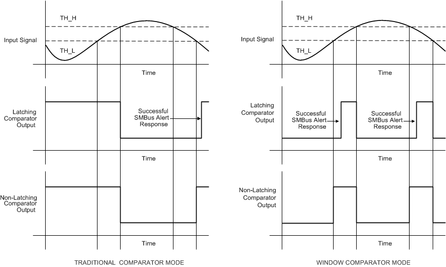
ADS1113 ADS1114 ADS1115 ai_tim_alert_comp_modes_bas444.gifFigure 28. ALERT Pin Timing Diagram
ADS1113 ADS1114 ADS1115 ai_tim_dout_reset_bas444.gifFigure 29. Conversion Ready Pulse in Continuous-Conversion Mode