JAJSF20B October   2017  – October 2018 ADS122C04

PRODUCTION DATA.  

  1. 特長
  2. アプリケーション
  3. 概要
    1.     Device Images
      1.      Kタイプ熱電対温度の測定
  4. 改訂履歴
  5. 概要(続き)
  6. Pin Configuration and Functions
    1.     Pin Functions
  7. Specifications
    1. 7.1 Absolute Maximum Ratings
    2. 7.2 ESD Ratings
    3. 7.3 Recommended Operating Conditions
    4. 7.4 Thermal Information
    5. 7.5 Electrical Characteristics
    6. 7.6 I2C Timing Requirements
    7. 7.7 I2C Switching Characteristics
    8. 7.8 Typical Characteristics
  8. Parameter Measurement Information
    1. 8.1 Noise Performance
  9. Detailed Description
    1. 9.1 Overview
    2. 9.2 Functional Block Diagram
    3. 9.3 Feature Description
      1. 9.3.1  Multiplexer
      2. 9.3.2  Low-Noise Programmable Gain Stage
        1. 9.3.2.1 PGA Input Voltage Requirements
        2. 9.3.2.2 Bypassing the PGA
      3. 9.3.3  Voltage Reference
      4. 9.3.4  Modulator and Internal Oscillator
      5. 9.3.5  Digital Filter
      6. 9.3.6  Conversion Times
      7. 9.3.7  Excitation Current Sources
      8. 9.3.8  Sensor Detection
      9. 9.3.9  System Monitor
      10. 9.3.10 Temperature Sensor
        1. 9.3.10.1 Converting From Temperature to Digital Codes
          1. 9.3.10.1.1 For Positive Temperatures (For Example, 50°C):
          2. 9.3.10.1.2 For Negative Temperatures (For Example, –25°C):
        2. 9.3.10.2 Converting From Digital Codes to Temperature
      11. 9.3.11 Offset Calibration
      12. 9.3.12 Conversion Data Counter
      13. 9.3.13 Data Integrity Features
    4. 9.4 Device Functional Modes
      1. 9.4.1 Power-Up and Reset
        1. 9.4.1.1 Power-On Reset
        2. 9.4.1.2 RESET Pin
        3. 9.4.1.3 Reset by Command
      2. 9.4.2 Conversion Modes
        1. 9.4.2.1 Single-Shot Conversion Mode
        2. 9.4.2.2 Continuous Conversion Mode
      3. 9.4.3 Operating Modes
        1. 9.4.3.1 Normal Mode
        2. 9.4.3.2 Turbo Mode
        3. 9.4.3.3 Power-Down Mode
    5. 9.5 Programming
      1. 9.5.1 I2C Interface
        1. 9.5.1.1 I2C Address
        2. 9.5.1.2 Serial Clock (SCL) and Serial Data (SDA)
        3. 9.5.1.3 Data Ready (DRDY)
        4. 9.5.1.4 Interface Speed
        5. 9.5.1.5 Data Transfer Protocol
        6. 9.5.1.6 I2C General Call (Software Reset)
        7. 9.5.1.7 Timeout
      2. 9.5.2 Data Format
      3. 9.5.3 Commands
        1. 9.5.3.1 Command Latching
        2. 9.5.3.2 RESET (0000 011x)
        3. 9.5.3.3 START/SYNC (0000 100x)
        4. 9.5.3.4 POWERDOWN (0000 001x)
        5. 9.5.3.5 RDATA (0001 xxxx)
        6. 9.5.3.6 RREG (0010 rrxx)
        7. 9.5.3.7 WREG (0100 rrxx dddd dddd)
      4. 9.5.4 Reading Data and Monitoring for New Conversion Results
      5. 9.5.5 Data Integrity
    6. 9.6 Register Map
      1. 9.6.1 Configuration Registers
      2. 9.6.2 Register Descriptions
        1. 9.6.2.1 Configuration Register 0 (address = 00h) [reset = 00h]
          1. Table 19. Configuration Register 0 Field Descriptions
        2. 9.6.2.2 Configuration Register 1 (address = 01h) [reset = 00h]
          1. Table 20. Configuration Register 1 Field Descriptions
        3. 9.6.2.3 Configuration Register 2 (address = 02h) [reset = 00h]
          1. Table 22. Configuration Register 2 Field Descriptions
        4. 9.6.2.4 Configuration Register 3 (address = 03h) [reset = 00h]
          1. Table 23. Configuration Register 3 Field Descriptions
  10. 10Application and Implementation
    1. 10.1 Application Information
      1. 10.1.1 Interface Connections
      2. 10.1.2 Connecting Multiple Devices on the Same I2C Bus
      3. 10.1.3 Unused Inputs and Outputs
      4. 10.1.4 Analog Input Filtering
      5. 10.1.5 External Reference and Ratiometric Measurements
      6. 10.1.6 Establishing Proper Limits on the Absolute Input Voltage
      7. 10.1.7 Pseudo Code Example
    2. 10.2 Typical Applications
      1. 10.2.1 K-Type Thermocouple Measurement (–200°C to +1250°C)
        1. 10.2.1.1 Design Requirements
        2. 10.2.1.2 Detailed Design Procedure
        3. 10.2.1.3 Application Curves
      2. 10.2.2 3-Wire RTD Measurement (–200°C to +850°C)
        1. 10.2.2.1 Design Requirements
        2. 10.2.2.2 Detailed Design Procedure
          1. 10.2.2.2.1 Design Variations for 2-Wire and 4-Wire RTD Measurements
        3. 10.2.2.3 Application Curves
      3. 10.2.3 Resistive Bridge Measurement
        1. 10.2.3.1 Design Requirements
        2. 10.2.3.2 Detailed Design Procedure
  11. 11Power Supply Recommendations
    1. 11.1 Power-Supply Sequencing
    2. 11.2 Power-Supply Decoupling
  12. 12Layout
    1. 12.1 Layout Guidelines
    2. 12.2 Layout Example
  13. 13デバイスおよびドキュメントのサポート
    1. 13.1 デバイス・サポート
      1. 13.1.1 デベロッパー・ネットワークの製品に関する免責事項
    2. 13.2 ドキュメントのサポート
      1. 13.2.1 関連資料
    3. 13.3 ドキュメントの更新通知を受け取る方法
    4. 13.4 コミュニティ・リソース
    5. 13.5 商標
    6. 13.6 静電気放電に関する注意事項
    7. 13.7 Glossary
  14. 14メカニカル、パッケージ、および注文情報

パッケージ・オプション

メカニカル・データ(パッケージ|ピン)
サーマルパッド・メカニカル・データ
発注情報

Interface Connections

Figure 68 shows the principle interface connections for the ADS122C04.
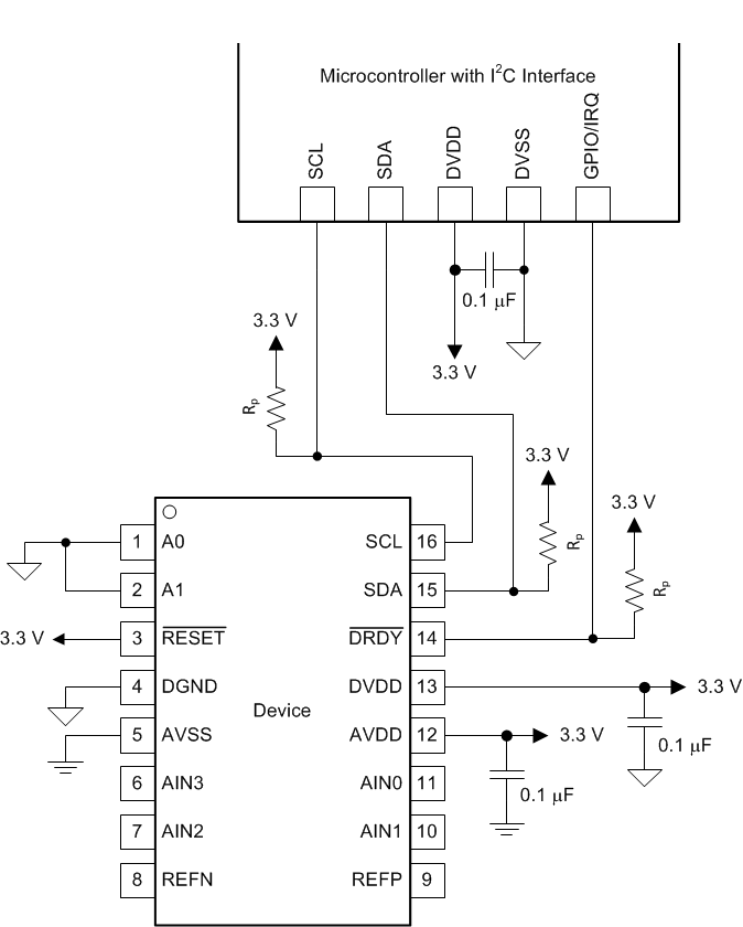
ADS122C04 ai_mcu_connection_bas751.gifFigure 68. Interface Connections

The ADS122C04 interfaces directly to standard-mode, fast-mode, or fast-mode plus I2C controllers. Any microcontroller I2C peripheral, including master-only and single-master I2C peripherals, operates with the ADS122C04. Details of the I2C communication protocol of the device can be found in the Programming section. The ADS122C04 does not perform clock-stretching (that is, the device never pulls the clock line low), so this function does not need to be provided for unless other clock-stretching devices are present on the same I2C bus.

Pullup resistors are required on both the SDA and SCL lines, as well as on the open-drain DRDY output. The size of these resistors depends on the bus operating speed and capacitance of the bus lines. Higher-value resistors yield lower power consumption when the bus lines are pulled low, but increase the transition times on the bus, which limits the bus speed. Lower-value resistors allow higher interface speeds, but at the expense of higher power consumption when the bus lines are pulled low. Long bus lines have higher capacitance and require smaller pullup resistors to compensate. Do not use resistors that are too small because the bus drivers may be unable to pull the bus lines low. See the I2C-Bus Specification and User Manual for details on pullup resistor sizing.