SBAS590E March 2016 – June 2020 ADS131A02 , ADS131A04
PRODUCTION DATA.
- 1 Features
- 2 Applications
- 3 Description
- 4 Revision History
- 5 Device Comparison Table
- 6 Pin Configuration and Functions
-
7 Specifications
- 7.1 Absolute Maximum Ratings
- 7.2 ESD Ratings
- 7.3 Recommended Operating Conditions
- 7.4 Thermal Information
- 7.5 Electrical Characteristics
- 7.6 Timing Requirements: Asynchronous Interrupt Interface Mode
- 7.7 Switching Characteristics: Asynchronous Interrupt Interface Mode
- 7.8 Timing Requirements: Synchronous Master Interface Mode
- 7.9 Switching Characteristics: Synchronous Master Interface Mode
- 7.10 Timing Requirements: Synchronous Slave Interface Mode
- 7.11 Switching Characteristics: Synchronous Slave Interface Mode
- 7.12 Typical Characteristics
- 8 Parameter Measurement Information
-
9 Detailed Description
- 9.1 Overview
- 9.2 Functional Block Diagram
- 9.3 Feature Description
- 9.4 Device Functional Modes
- 9.5
Programming
- 9.5.1 Interface Protocol
- 9.5.2 SPI Interface
- 9.5.3
SPI Command Definitions
- 9.5.3.1 NULL: Null Command
- 9.5.3.2 RESET: Reset to POR Values
- 9.5.3.3 STANDBY: Enter Standby Mode
- 9.5.3.4 WAKEUP: Exit Standby Mode
- 9.5.3.5 LOCK: Lock ADC Registers
- 9.5.3.6 UNLOCK: Unlock ADC Registers
- 9.5.3.7 RREG: Read a Single Register
- 9.5.3.8 RREGS: Read Multiple Registers
- 9.5.3.9 WREG: Write Single Register
- 9.5.3.10 WREGS: Write Multiple Registers
- 9.6
Register Maps
- 9.6.1
User Register Description
- 9.6.1.1 ID_MSB: ID Control Register MSB (address = 00h) [reset = xxh]
- 9.6.1.2 ID_LSB: ID Control Register LSB (address = 01h) [reset = xxh]
- 9.6.1.3 STAT_1: Status 1 Register (address = 02h) [reset = 00h]
- 9.6.1.4 STAT_P: Positive Input Fault Detect Status Register (address = 03h) [reset = 00h]
- 9.6.1.5 STAT_N: Negative Input Fault Detect Status Register (address = 04h) [reset = 00h]
- 9.6.1.6 STAT_S: SPI Status Register (address = 05h) [reset = 00h]
- 9.6.1.7 ERROR_CNT: Error Count Register (address = 06h) [reset = 00h]
- 9.6.1.8 STAT_M2: Hardware Mode Pin Status Register (address = 07h) [reset = xxh]
- 9.6.1.9 Reserved Registers (address = 08h to 0Ah) [reset = 00h]
- 9.6.1.10 A_SYS_CFG: Analog System Configuration Register (address = 0Bh) [reset = 60h]
- 9.6.1.11 D_SYS_CFG: Digital System Configuration Register (address = 0Ch) [reset = 3Ch]
- 9.6.1.12 CLK1: Clock Configuration 1 Register (address = 0Dh) [reset = 08h]
- 9.6.1.13 CLK2: Clock Configuration 2 Register (address = 0Eh) [reset = 86h]
- 9.6.1.14 ADC_ENA: ADC Channel Enable Register (address = 0Fh) [reset = 00h]
- 9.6.1.15 Reserved Register (address = 10h) [reset = 00h]
- 9.6.2 ADCx: ADC Channel Digital Gain Configuration Registers (address = 11h to 14h) [reset = 00h]
- 9.6.1
User Register Description
- 10Application and Implementation
- 11Power Supply Recommendations
- 12Layout
- 13Device and Documentation Support
- 14Mechanical, Packaging, and Orderable Information
パッケージ・オプション
デバイスごとのパッケージ図は、PDF版データシートをご参照ください。
メカニカル・データ(パッケージ|ピン)
- PBS|32
サーマルパッド・メカニカル・データ
- PBS|32
発注情報
9.3.4 Reference
The ADS131A0x offers an integrated low-drift, 2.442-V or 4.0-V reference option. For applications that require a different reference voltage, the device offers a reference input option for use with an external reference voltage.
The reference source is selected by the INT_REFEN bit in the A_SYS_CFG register. By default, the external reference is selected (INT_REFEN = 0). The internal voltage reference requires 0.2 ms to settle to 1% and 250 ms to fully settle to 0.01% when switching from an external reference source to the internal reference (using the recommended bypass capacitor values). The external reference input is internally buffered to increase input impedance. Therefore, additional reference buffers are usually not required when using an external reference. Connect the reference voltage to the REFEXT pin when using an external reference.
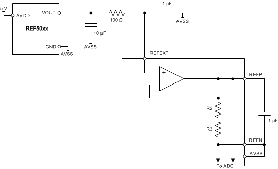
External band-limiting capacitors determine the amount of reference noise contribution. For high-end systems, choose capacitor values such that the bandwidth is limited to less than 10 Hz so that the reference noise does not dominate the system noise. In systems with strict ADC power-on requirements, using a large capacitor on the reference increases the time for the voltage to meet the desired value, thus increasing system power-on time. Figure 43 illustrates a typical external reference drive circuitry with recommended filtering options.
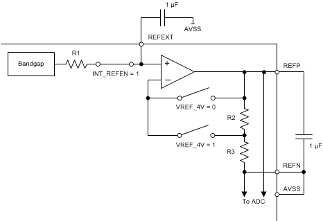
Set the INTREF_EN bit to 1 in the A_SYS_CFG register to use the internal reference. When the internal reference is selected, use the VREF_4V bit to select between a 2.442-V or 4.0-V reference. By default, the device is set to use the 2.442-V reference. The VREF_4V bit has no function when set to use the external reference. When enabling the negative charge pump with a 3.0-V to 3.45-V analog supply, the internal reference must be set to 2.442 V. Figure 44 shows a simplified block diagram of the internal ADS131A0x reference. The reference voltage is generated with respect to AVSS requiring a direct connection between REFN and AVSS.

