SBAS456B December 2008 – January 2016 ADS7828-Q1
PRODUCTION DATA.
- 1 Features
- 2 Applications
- 3 Description
- 4 Revision History
- 5 Pin Configuration and Functions
-
6 Specifications
- 6.1 Absolute Maximum Ratings
- 6.2 ESD Ratings
- 6.3 Recommended Operating Conditions
- 6.4 Thermal Information
- 6.5 Electrical Characteristics for ADS7828E
- 6.6 Electrical Characteristics for ADS7828EB
- 6.7 Electrical Characteristics for ADS7828E
- 6.8 Electrical Characteristics for ADS7828EB
- 6.9 Switching Characteristics
- 6.10 Typical Characteristics
- 7 Detailed Description
- 8 Application and Implementation
- 9 Power Supply Recommendations
- 10Layout
- 11Device and Documentation Support
- 12Mechanical, Packaging, and Orderable Information
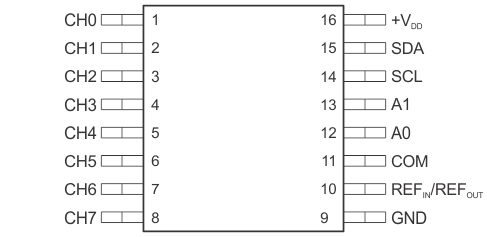
5 Pin Configuration and Functions
PW Package
16-Pin TSSOP
Top View

Pin Functions
| PIN | DESCRIPTION | |
|---|---|---|
| NO. | NAME | |
| 1 | CH0 | Differential channel 0: positive input or single-ended channel 0 input |
| 2 | CH1 | Differential channel 0: negative input or single-ended channel 1 input |
| 3 | CH2 | Differential channel 1: positive input or single-ended channel 2 input |
| 4 | CH3 | Differential channel 1: negative input or single-ended channel 3 input |
| 5 | CH4 | Differential channel 2: positive input or single-ended channel 4 input |
| 6 | CH5 | Differential channel 2: negative input or single-ended channel 5 input |
| 7 | CH6 | Differential channel 3: positive input or single-ended channel 6 input |
| 8 | CH7 | Differential channel 3: negative input or single-ended channel 7 input |
| 9 | GND | Analog ground |
| 10 | REFIN / REFOUT | Internal 2.5-V reference / external reference input |
| 11 | COM | Common to analog input channel |
| 12 | A0 | Slave address bit 0 |
| 13 | A1 | Slave address bit 1 |
| 14 | SCL | Serial clock |
| 15 | SDA | Serial data |
| 16 | +VDD | Power supply, 3.3 V (nominal) |