JAJSHX7A September 2010 – September 2019 ADS7947 , ADS7948 , ADS7949
PRODUCTION DATA.
- 1 特長
- 2 アプリケーション
- 3 概要
- 4 改訂履歴
- 5 Device Comparison Table
- 6 Pin Configuration and Functions
-
7 Specifications
- 7.1 Absolute Maximum Ratings
- 7.2 ESD Ratings
- 7.3 Recommended Operating Conditions: ADS794x (12-, 10-, 8-Bit)
- 7.4 Thermal Information
- 7.5 Electrical Characteristics: ADS7947 (12-Bit)
- 7.6 Electrical Characteristics: ADS7948 (10-Bit)
- 7.7 Electrical Characteristics: ADS7949 (8-Bit)
- 7.8 Timing Requirements
- 7.9 Switching Characteristics
- 7.10 Typical Characteristics: ADS7947, ADS7948, ADS7949
- 7.11 Typical Characteristics: ADS7947 (12-Bit)
- 8 Detailed Description
- 9 Application and Implementation
- 10Power Supply Recommendations
- 11Layout
- 12デバイスおよびドキュメントのサポート
- 13メカニカル、パッケージ、および注文情報
パッケージ・オプション
メカニカル・データ(パッケージ|ピン)
- RTE|16
サーマルパッド・メカニカル・データ
- RTE|16
発注情報
8.3.5 Power-Down
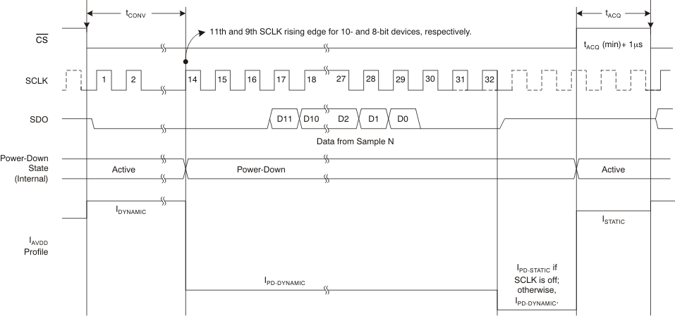
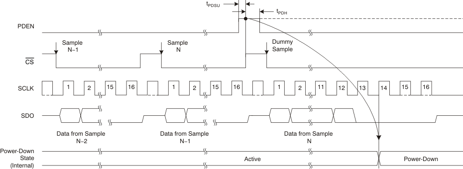
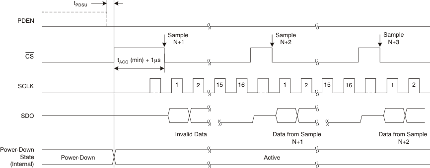
The ADS7947, ADS7948, and ADS7949 family of devices offers an easy-to-use power-down feature available through a dedicated PDEN pin (pin 12). A high level on PDEN at the CS rising edge enables the power-down mode for that particular cycle. Figure 44 to Figure 46 illustrate device operation with power-down in both 32-clock and 16-clock mode.
Many applications must slow device operation. For speeds below approximately 500 kSPS, the 32-clock mode can be used with power-down. This capability results in considerable power savings.
As illustrated in Figure 44, PDEN is held at a logic '1' level. The device observes the PDEN status only at the CS rising edge; however, for continuous low-speed operation, continuously hold PDEN = 1. The devices detect power-down mode on the CS rising edge with PDEN = 1.
 Figure 44. Operation With a 32-Clock Frame in Power-Down Mode (PDEN = 1)
 On the CS falling edge, the devices start normal operation as previously described. The devices complete conversions on the 14th SCLK rising edge. (Conversions complete on the 11th and ninth SCLK rising edge for 10-bit and 8-bit devices, respectively.) The devices enter the power-down state immediately after conversions complete. However, the devices can still output data as per the timings described previously. The devices consume dynamic power-down current (IPD-DYNAMIC) during data out operations. TI recommends stopping the clock after the 32nd SCLK falling edge to further save power down to the static power-down current level (IPD-STATIC). The devices power up again on the SCLK rising edge. However, they require an extra 1µs to power up completely. CS must be high for the 1µs + tACQ (min) period.
In some applications, data collection is accomplished in burst mode. The system powers down after data collection. 16-clock mode is convenient for these applications. Figure 45 and Figure 46 detail power saving in 16-clock burst mode.
As illustrated in Figure 45, the two frames capturing the N–1 and Nth samples are normal 16-clock frames. Keeping PDEN = 1 prior to the CS rising edge in the next frame ensures that the devices detect the power-down mode. Data from the Nth sample are read during this frame. The Nth sample represents the last data of interest in the burst of conversions. The devices enter power-down state after the end of conversions. This state is the 14th, 11th, or ninth SCLK rising edge for the 12-, 10-, and 8-bit devices, respectively. The clock can be stopped after the 14th SCLK falling edge; however, TI still recommends stopping the clock after the 16th SCLK falling edge. There must be no more than 29 SCLK falling edges during the CS low period. This limitation ensures that the devices remain in 16-clock mode.
The devices remain in a power-down state as long as CS is low. A CS rising edge with PDEN = 0 brings the devices out of the power-down state. Ensure that the CS high time for the first sample after power up is more than 1 µs + tACQ (min).
 Figure 45. Entry Into Power-Down With 16-Clock Burst Mode
  Figure 46. Exit From Power-Down With 16-Clock Burst Mode