JAJSDP7 August 2017 AM5718-HIREL
PRODUCTION DATA.
- 1 デバイスの概要
- 2 改訂履歴
- 3 Device Comparison
-
4 Terminal Configuration and Functions
- 4.1 Terminal Assignment
- 4.2 Ball Characteristics
- 4.3 Multiplexing Characteristics
- 4.4
Signal Descriptions
- 4.4.1 Video Input Ports (VIP)
- 4.4.2 Display Subsystem - Video Output Ports
- 4.4.3 Display Subsystem - High-Definition Multimedia Interface (HDMI)
- 4.4.4 Camera Serial Interface 2 CAL bridge (CSI2)
- 4.4.5 External Memory Interface (EMIF)
- 4.4.6 General-Purpose Memory Controller (GPMC)
- 4.4.7 Timers
- 4.4.8 Inter-Integrated Circuit Interface (I2C)
- 4.4.9 HDQ / 1-Wire Interface (HDQ1W)
- 4.4.10 Universal Asynchronous Receiver Transmitter (UART)
- 4.4.11 Multichannel Serial Peripheral Interface (McSPI)
- 4.4.12 Quad Serial Peripheral Interface (QSPI)
- 4.4.13 Multichannel Audio Serial Port (McASP)
- 4.4.14 Universal Serial Bus (USB)
- 4.4.15 SATA
- 4.4.16 Peripheral Component Interconnect Express (PCIe)
- 4.4.17 Controller Area Network Interface (DCAN)
- 4.4.18 Ethernet Interface (GMAC_SW)
- 4.4.19 Media Local Bus (MLB) Interface
- 4.4.20 eMMC/SD/SDIO
- 4.4.21 General-Purpose Interface (GPIO)
- 4.4.22 Keyboard controller (KBD)
- 4.4.23 Pulse Width Modulation (PWM) Interface
- 4.4.24 Programmable Real-Time Unit Subsystem and Industrial Communication Subsystem (PRU-ICSS)
- 4.4.25 Test Interfaces
- 4.4.26 System and Miscellaneous
- 4.4.27 Power Supplies
-
5 Specifications
- 5.1 Absolute Maximum Ratings
- 5.2 ESD Ratings
- 5.3 Power On Hours (POH) Limits
- 5.4 Recommended Operating Conditions
- 5.5 Operating Performance Points
- 5.6 Power Consumption Summary
- 5.7
Electrical Characteristics
- 5.7.1 LVCMOS DDR DC Electrical Characteristics
- 5.7.2 HDMIPHY DC Electrical Characteristics
- 5.7.3 Dual Voltage LVCMOS I2C DC Electrical Characteristics
- 5.7.4 IQ1833 Buffers DC Electrical Characteristics
- 5.7.5 IHHV1833 Buffers DC Electrical Characteristics
- 5.7.6 LVCMOS OSC Buffers DC Electrical Characteristics
- 5.7.7 LVCMOS CSI2 DC Electrical Characteristics
- 5.7.8 BMLB18 Buffers DC Electrical Characteristics
- 5.7.9 BC1833IHHV Buffers DC Electrical Characteristics
- 5.7.10 USBPHY DC Electrical Characteristics
- 5.7.11 Dual Voltage SDIO1833 DC Electrical Characteristics
- 5.7.12 Dual Voltage LVCMOS DC Electrical Characteristics
- 5.7.13 SATAPHY DC Electrical Characteristics
- 5.7.14 SERDES DC Electrical Characteristics
- 5.8 Thermal Characteristics
- 5.9 Power Supply Sequences
- 6 Clock Specifications
-
7 Timing Requirements and Switching Characteristics
- 7.1 Timing Test Conditions
- 7.2 Interface Clock Specifications
- 7.3 Timing Parameters and Information
- 7.4 Recommended Clock and Control Signal Transition Behavior
- 7.5 Virtual and Manual I/O Timing Modes
- 7.6 Video Input Ports (VIP)
- 7.7 Display Subsystem - Video Output Ports
- 7.8 Display Subsystem - High-Definition Multimedia Interface (HDMI)
- 7.9 Camera Serial Interface 2 CAL bridge (CSI2)
- 7.10 External Memory Interface (EMIF)
- 7.11 General-Purpose Memory Controller (GPMC)
- 7.12 Timers
- 7.13 Inter-Integrated Circuit Interface (I2C)
- 7.14 HDQ / 1-Wire Interface (HDQ1W)
- 7.15 Universal Asynchronous Receiver Transmitter (UART)
- 7.16 Multichannel Serial Peripheral Interface (McSPI)
- 7.17 Quad Serial Peripheral Interface (QSPI)
- 7.18 Multichannel Audio Serial Port (McASP)
- 7.19 Universal Serial Bus (USB)
- 7.20 Serial Advanced Technology Attachment (SATA)
- 7.21 Peripheral Component Interconnect Express (PCIe)
- 7.22 Controller Area Network Interface (DCAN)
- 7.23 Ethernet Interface (GMAC_SW)
- 7.24
eMMC/SD/SDIO
- 7.24.1
MMC1-SD Card Interface
- 7.24.1.1 Default speed, 4-bit data, SDR, half-cycle
- 7.24.1.2 High speed, 4-bit data, SDR, half-cycle
- 7.24.1.3 SDR12, 4-bit data, half-cycle
- 7.24.1.4 SDR25, 4-bit data, half-cycle
- 7.24.1.5 UHS-I SDR50, 4-bit data, half-cycle
- 7.24.1.6 UHS-I SDR104, 4-bit data, half-cycle
- 7.24.1.7 UHS-I DDR50, 4-bit data
- 7.24.2 MMC2 - eMMC
- 7.24.3 MMC3 and MMC4-SDIO/SD
- 7.24.1
MMC1-SD Card Interface
- 7.25 General-Purpose Interface (GPIO)
- 7.26 PRU-ICSS Interfaces
- 7.27 System and Miscellaneous interfaces
- 7.28 Test Interfaces
-
8 Applications, Implementation, and Layout
- 8.1 Power Supply Mapping
- 8.2
DDR3 Board Design and Layout Guidelines
- 8.2.1 DDR3 General Board Layout Guidelines
- 8.2.2
DDR3 Board Design and Layout Guidelines
- 8.2.2.1 Board Designs
- 8.2.2.2 DDR3 EMIF
- 8.2.2.3 DDR3 Device Combinations
- 8.2.2.4 DDR3 Interface Schematic
- 8.2.2.5 Compatible JEDEC DDR3 Devices
- 8.2.2.6 PCB Stackup
- 8.2.2.7 Placement
- 8.2.2.8 DDR3 Keepout Region
- 8.2.2.9 Bulk Bypass Capacitors
- 8.2.2.10 High-Speed Bypass Capacitors
- 8.2.2.11 Net Classes
- 8.2.2.12 DDR3 Signal Termination
- 8.2.2.13 VREF_DDR Routing
- 8.2.2.14 VTT
- 8.2.2.15 CK and ADDR_CTRL Topologies and Routing Definition
- 8.2.2.16 Data Topologies and Routing Definition
- 8.2.2.17 Routing Specification
- 8.3 High Speed Differential Signal Routing Guidance
- 8.4 Power Distribution Network Implementation Guidance
- 8.5 Single-Ended Interfaces
- 8.6 Clock Routing Guidelines
- 9 デバイスおよびドキュメントのサポート
- 10メカニカル、パッケージ、および注文情報
6 Clock Specifications
NOTE
For more information, see Power, Reset, and Clock Management / PRCM Environment / External Clock Signal and Power Reset / PRCM Functional Description / PRCM Clock Manager Functional Description section of the Device TRM.
NOTE
Audio Back End (ABE) module is not supported for this family of devices, but “ABE” name is still present in some clock or DPLL names.
The device operation requires the following clocks:
- The 32 kHz frequency is used for low frequency operation. It supplies the wake-up domain for operation in lowest power mode. This is an optional clock and will be supplied by on chip divider + mux (FUNC_32K_CLK) incase it is not available on external pin.
- The system clocks, SYS_CLKIN1(Mandatory) and SYS_CLKIN2(Optional) are the main clock sources of the device. They supply the reference clock to the DPLLs as well as functional clock to several modules.
The Device also embeds an internal free-running 32-kHz oscillator that is always active as long as the the wake-up (WKUP) domain is supplied.
Figure 6-1 shows the external input clock sources and the output clocks to peripherals.
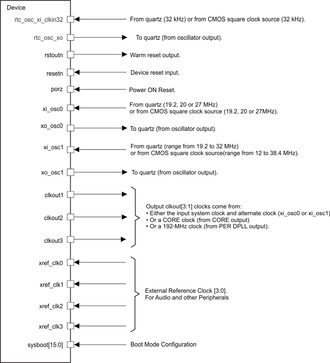 Figure 6-1 Clock Interface
6.1 Input Clock Specifications
6.1.1 Input Clock Requirements
- The source of the internal system clock (SYS_CLK1) could be either:
- A CMOS clock that enters on the xi_osc0 ball (with xo_osc0 left unconnected on the CMOS clock case).
- A crystal oscillator clock managed by xi_osc0 and xo_osc0.
- The source of the internal system clock (SYS_CLK2) could be either:
- A CMOS clock that enters on the xi_osc1 ball (with xo_osc1 left unconnected on the CMOS clock case).
- A crystal oscillator clock managed by xi_osc1 and xo_osc1.
- The source of the internal system clock (SYS_32K) could be either:
- A CMOS clock that enters on the rtc_osc_xi_clkin32 ball and supports external LVCMOS clock generators
- A crystal oscillator clock managed by rtc_osc_xi_clkin32 and rtc_osc_xo.
6.1.2 System Oscillator OSC0 Input Clock
SYS_CLKIN1 is received directly from oscillator OSC0. For more information about SYS_CLKIN1 see Device TRM, Chapter: Power, Reset, and Clock Management.
6.1.2.1 OSC0 External Crystal
An external crystal is connected to the device pins. Figure 6-2 describes the crystal implementation.
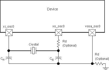 Figure 6-2 Crystal Implementation
NOTE
The load capacitors,Cf1 and Cf2 in Figure 6-2, should be chosen such that the below equation is satisfied. CL in the equation is the load specified by the crystal manufacturer. All discrete components used to implement the oscillator circuit should be placed as close as possible to the associated oscillator xi_osc0, xo_osc0, and vssa_osc0 pins.
 Figure 6-3 Load Capacitance Equation
The crystal must be in the fundamental mode of operation and parallel resonant. Table 6-1 summarizes the required electrical constraints.
Table 6-1 OSC0 Crystal Electrical Characteristics
| NAME | DESCRIPTION | MIN | TYP | MAX | UNIT | ||
|---|---|---|---|---|---|---|---|
| fp | Parallel resonance crystal frequency | 19.2, 20, 27 | MHz | ||||
| Cf1 | Cf1 load capacitance for crystal parallel resonance with Cf1 = Cf2 | 12 | 24 | pF | |||
| Cf2 | Cf2 load capacitance for crystal parallel resonance with Cf1 = Cf2 | 12 | 24 | pF | |||
| ESR(Cf1,Cf2) (1) | Crystal ESR | 100 | Ω | ||||
| CO | Crystal shunt capacitance | ESR = 30 Ω ESR = 40 Ω |
19.2 MHz, 20 MHz, 27 MHz | 7 | pF | ||
| ESR = 50 Ω | 19.2 MHz, 20 MHz | 7 | pF | ||||
| 27 MHz | 5 | pF | |||||
| ESR = 60 Ω | 19.2 MHz, 20 MHz | 7 | pF | ||||
| 27 MHz | Not Supported | - | |||||
| ESR = 80 Ω | 19.2 MHz, 20 MHz | 5 | pF | ||||
| 27 MHz | Not Supported | - | |||||
| ESR = 100 Ω | 19.2 MHz, 20 MHz | 3 | pF | ||||
| 27 MHz | Not Supported | - | |||||
| LM | Crystal motional inductance for fp = 20 MHz | 10.16 | mH | ||||
| CM | Crystal motional capacitance | 3.42 | fF | ||||
| tj(xiosc0) | Frequency accuracy (1), xi_osc0 | Ethernet not used | ±200 | ppm | |||
| Ethernet RGMII and RMII using derived clock | ±50 | ||||||
| Ethernet MII using derived clock | ±100 | ||||||
- Crystal characteristics should account for tolerance+stability+aging.
When selecting a crystal, the system design must take into account the temperature and aging characteristics of a crystal versus the user environment and expected lifetime of the system.
Table 6-2 details the switching characteristics of the oscillator and the requirements of the input clock.
Table 6-2 Oscillator Switching Characteristics—Crystal Mode
| NAME | DESCRIPTION | MIN | TYP | MAX | UNIT |
|---|---|---|---|---|---|
| fp | Oscillation frequency | 19.2, 20, 27 MHz | MHz | ||
| tsX | Start-up time | 4 | ms | ||
6.1.2.2 OSC0 Input Clock
A 1.8-V LVCMOS-Compatible Clock Input can be used instead of the internal oscillator to provide the SYS_CLKIN1 clock input to the system. The external connections to support this are shown in Figure 6-4. The xi_osc0 pin is connected to the 1.8-V LVCMOS-Compatible clock source. The xi_osc0 pin is left unconnected. The vssa_osc0 pin is connected to board ground (VSS).
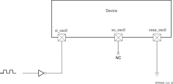 Figure 6-4 1.8-V LVCMOS-Compatible Clock Input
Table 6-3 summarizes the OSC0 input clock electrical characteristics.
Table 6-3 OSC0 Input Clock Electrical Characteristics—Bypass Mode
| NAME | DESCRIPTION | MIN | TYP | MAX | UNIT |
|---|---|---|---|---|---|
| f | Frequency | 19.2, 20, 27 | MHz | ||
| CIN | Input capacitance | 2.184 | 2.384 | 2.584 | pF |
| IIN | Input current (3.3V mode) | 4 | 6 | 10 | µA |
Table 6-4 details the OSC0 input clock timing requirements.
Table 6-4 OSC0 Input Clock Timing Requirements
| NAME | DESCRIPTION | MIN | TYP | MAX | UNIT | ||
|---|---|---|---|---|---|---|---|
| CK0 | 1 / tc(xiosc0) | Frequency, xi_osc0 | 19.2, 20, 27 | MHz | |||
| CK1 | tw(xiosc0) | Pulse duration, xi_osc0 low or high |
0.45 * tc(xiosc0) |
0.55 * tc(xiosc0) | ns | ||
| tj(xiosc0) | Period jitter(1), xi_osc0 | 0.01 × tc(xiosc0) | ns | ||||
| tR(xiosc0) | Rise time, xi_osc0 | 5 | ns | ||||
| tF(xiosc0) | Fall time, xi_osc0 | 5 | ns | ||||
| tj(xiosc0) | Frequency accuracy(4), xi_osc0 | Ethernet not used | ±200 | ppm | |||
| Ethernet RGMII and RMII using derived clock | ±50 | ||||||
| Ethernet MII using derived clock | ±100 | ||||||
- Period jitter is meant here as follows:
- Crystal characteristics should account for tolerance+stability+aging.
– The maximum value is the difference between the longest measured clock period and the expected clock period
– The minimum value is the difference between the shortest measured clock period and the expected clock period
 Figure 6-5 xi_osc0 Input Clock
6.1.3 Auxiliary Oscillator OSC1 Input Clock
SYS_CLKIN2 is received directly from oscillator OSC1. For more information about SYS_CLKIN2 see Device TRM, Chapter: Power, Reset, and Clock Management.
6.1.3.1 OSC1 External Crystal
An external crystal is connected to the device pins. Figure 6-6 describes the crystal implementation.
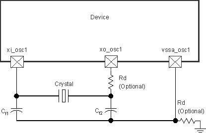 Figure 6-6 Crystal Implementation
NOTE
The load capacitors, Cf1 and Cf2 in Figure 6-6, should be chosen such that the below equation is satisfied. CL in the equation is the load specified by the crystal manufacturer. All discrete components used to implement the oscillator circuit should be placed as close as possible to the associated oscillator xi_osc1, xo_osc1, and vssa_osc1 pins.
 Figure 6-7 Load Capacitance Equation
The crystal must be in the fundamental mode of operation and parallel resonant. Table 6-5 summarizes the required electrical constraints.
Table 6-5 OSC1 Crystal Electrical Characteristics
| NAME | DESCRIPTION | MIN | TYP | MAX | UNIT | ||
|---|---|---|---|---|---|---|---|
| fp | Parallel resonance crystal frequency | Range from 19.2 to 32 | MHz | ||||
| Cf1 | Cf1 load capacitance for crystal parallel resonance with Cf1 = Cf2 | 12 | 24 | pF | |||
| Cf2 | Cf2 load capacitance for crystal parallel resonance with Cf1 = Cf2 | 12 | 24 | pF | |||
| ESR(Cf1,Cf2) | Crystal ESR | 100 | Ω | ||||
| CO | Crystal shunt capacitance | ESR = 30 Ω | 19.2 MHz ≤ fp ≤ 32 MHz | 7 | pF | ||
| ESR = 40 Ω | 19.2 MHz ≤ fp ≤ 32 MHz | 5 | pF | ||||
| ESR = 50 Ω | 19.2 MHz ≤ fp ≤ 25 MHz | 7 | pF | ||||
| 25 MHz < fp ≤ 27 MHz | 5 | pF | |||||
| 27 MHz < fp ≤ 32 MHz | Not Supported | - | |||||
| ESR = 60 Ω | 19.2 MHz ≤ fp ≤ 23 MHz | 7 | pF | ||||
| 23 MHz < fp ≤ 25 MHz | 5 | pF | |||||
| 25 MHz < fp ≤ 32 MHz | Not Supported | - | |||||
| ESR = 80 Ω | 19.2 MHz ≤ fp ≤ 23 MHz | 5 | pF | ||||
| 23 MHz ≤ fp ≤ 25 MHz | 3 | pF | |||||
| 25 MHz < fp ≤ 32 MHz | Not Supported | - | |||||
| ESR = 100 Ω | 19.2 MHz ≤ fp ≤ 20 MHz | 3 | pF | ||||
| 20 MHz < fp ≤ 32 MHz | Not Supported | - | |||||
| LM | Crystal motional inductance for fp = 20 MHz | 10.16 | mH | ||||
| CM | Crystal motional capacitance | 3.42 | fF | ||||
| tj(xiosc1) | Frequency accuracy(1), xi_osc1 | Ethernet not used | ±200 | ppm | |||
| Ethernet RGMII and RMII using derived clock | ±50 | ||||||
| Ethernet MII using derived clock | ±100 | ||||||
- Crystal characteristics should account for tolerance+stability+aging.
When selecting a crystal, the system design must take into account the temperature and aging characteristics of a crystal versus the user environment and expected lifetime of the system.
Table 6-6 details the switching characteristics of the oscillator and the requirements of the input clock.
Table 6-6 Oscillator Switching Characteristics—Crystal Mode
| NAME | DESCRIPTION | MIN | TYP | MAX | UNIT |
|---|---|---|---|---|---|
| fp | Oscillation frequency | Range from 19.2 to 32 | MHz | ||
| tsX | Start-up time | 4 | ms | ||
6.1.3.2 OSC1 Input Clock
A 1.8-V LVCMOS-Compatible Clock Input can be used instead of the internal oscillator to provide the SYS_CLKIN2 clock input to the system. The external connections to support this are shown in, Figure 6-8. The xi_osc1 pin is connected to the 1.8-V LVCMOS-Compatible clock sources. The xo_osc1 pin is left unconnected. The vssa_osc1 pin is connected to board ground (vss).
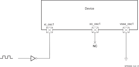 Figure 6-8 1.8-V LVCMOS-Compatible Clock Input
Table 6-7 summarizes the OSC1 input clock electrical characteristics.
Table 6-7 OSC1 Input Clock Electrical Characteristics—Bypass Mode
| NAME | DESCRIPTION | MIN | TYP | MAX | UNIT |
|---|---|---|---|---|---|
| f | Frequency | Range from 12 to 38.4 | MHz | ||
| CIN | Input capacitance | 2.819 | 3.019 | 3.219 | pF |
| IIN | Input current (3.3V mode) | 4 | 6 | 10 | µA |
| tsX | Start-up time(1) | See(2) | ms | ||
- To switch from bypass mode to crystal or from crystal mode to bypass mode, there is a waiting time about 100 μs; however, if the chip comes from bypass mode to crystal mode the crystal will start-up after time mentioned in Table 6-6, tsX parameter.
- Before the processor boots up and the oscillator is set to bypass mode, there is a waiting time when the internal oscillator is in application mode and receives a wave. The switching time in this case is about 100 μs.
Table 6-8 details the OSC1 input clock timing requirements.
Table 6-8 OSC1 Input Clock Timing Requirements
| NAME | DESCRIPTION | MIN | TYP | MAX | UNIT | ||
|---|---|---|---|---|---|---|---|
| CK0 | 1 / tc(xiosc1) | Frequency, xi_osc1 | Range from 12 to 38.4 | MHz | |||
| CK1 | tw(xiosc1) | Pulse duration, xi_osc1 low or high | 0.45 * tc(xiosc1) | 0.55 * tc(xiosc1) | ns | ||
| tj(xiosc1) | Period jitter(1), xi_osc1 | 0.01 × tc(xiosc1) (3) | ns | ||||
| tR(xiosc1) | Rise time, xi_osc1 | 5 | ns | ||||
| tF(xiosc1) | Fall time, xi_osc1 | 5 | ns | ||||
| tj(xiosc1) | Frequency accuracy(2), xi_osc1 | Ethernet not used | ±200 | ppm | |||
| Ethernet RGMII and RMII using derived clock | ±50 | ||||||
| Ethernet MII using derived clock | ±100 | ||||||
- Period jitter is meant here as follows:
- The maximum value is the difference between the longest measured clock period and the expected clock period
- The minimum value is the difference between the shortest measured clock period and the expected clock period
- Crystal characteristics should account for tolerance+stability+aging.
- The Period jitter requirement for osc1 can be relaxed to 0.02*tc(xiosc1) under the following constraints:
a.The osc1/SYS_CLK2 clock bypasses all device PLLs
b.The osc1/SYS_CLK2 clock is only used to source the DSS pixel clock outputs
 Figure 6-9 xi_osc1 Input Clock
6.1.4 RTC Oscillator Input Clock
SYS_32K is received directly from RTC Oscillator. For more information about SYS_32K see the Device TRM, Power, Reset, and Clock Management chapter.
NOTE
RTC only mode is not supported feature.
6.1.4.1 RTC Oscillator External Crystal
An external crystal is connected to the device pins. Figure 6-2 describes the crystal implementation.
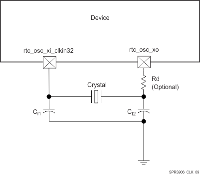 Figure 6-10 Crystal Implementation
NOTE
The load capacitors, Cf1 and Cf2 in Figure 6-10, should be chosen such that the below equation is satisfied. CL in the equation is the load specified by the crystal manufacturer. All discrete components used to implement the oscillator circuit should be placed as close as possible to the associated oscillator rtc_osc_xi_clkin32 and rtc_osc_xo pins.
 Figure 6-11 Load Capacitance Equation
The crystal must be in the fundamental mode of operation and parallel resonant. Table 6-9 summarizes the required electrical constraints.
Table 6-9 RTC Crystal Electrical Characteristics
| NAME | DESCRIPTION | MIN | TYP | MAX | UNIT |
|---|---|---|---|---|---|
| fp | Parallel resonance crystal frequency | 32.768 | kHz | ||
| Cf1 | Cf1 load capacitance for crystal parallel resonance with Cf1 = Cf2 | 12 | 24 | pF | |
| Cf2 | Cf2 load capacitance for crystal parallel resonance with Cf1 = Cf2 | 12 | 24 | pF | |
| ESR(Cf1,Cf2) | Crystal ESR | 80 | kΩ | ||
| CO | Crystal shunt capacitance | 5 | pF | ||
| LM | Crystal motional inductance for fp = 32.768 kHz | 10.7 | mH | ||
| CM | Crystal motional capacitance | 2.2 | fF | ||
| tj(rtc_osc_xi_clkin32) | Frequency accuracy, rtc_osc_xi_clkin32 | ±200 | ppm | ||
When selecting a crystal, the system design must take into account the temperature and aging characteristics of a crystal versus the user environment and expected lifetime of the system.
Table 6-10 details the switching characteristics of the oscillator and the requirements of the input clock.
Table 6-10 Oscillator Switching Characteristics—Crystal Mode
| NAME | DESCRIPTION | MIN | TYP | MAX | UNIT |
|---|---|---|---|---|---|
| fp | Oscillation frequency | 32.768 | kHz | ||
| tsX | Start-up time | 4 | ms | ||
6.1.4.2 RTC Oscillator Input Clock
A 1.8-V LVCMOS-Compatible Clock Input can be used instead of the internal oscillator to provide the SYS_32K clock input to the system. The external connections to support this are shown in Figure 6-12. The rtc_osc_xi_clkin32 pin is connected to the 1.8-V LVCMOS-Compatible clock sources. The rtc_osc_xo pin is left unconnected.
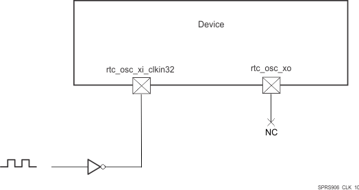 Figure 6-12 LVCMOS-Compatible Clock Input
Table 6-11 summarizes the RTC Oscillator input clock electrical characteristics.
Table 6-11 RTC Oscillator Input Clock Electrical Characteristics—Bypass Mode
| NAME | DESCRIPTION | MIN | TYP | MAX | UNIT | |
|---|---|---|---|---|---|---|
| CK0 | 1/tc(rtc_osc_xi_clkin32) | Frequency, rtc_osc_xi_clkin32 | 32.768 | kHz | ||
| CK1 | tw(rtc_osc_xi_clkin32) | Pulse duration, rtc_osc_xi_clkin32 low or high | 0.45 * tc(rtc_osc_xi_clkin32) | 0.55 * tc(rtc_osc_xi_clkin32) | ns | |
| CIN | Input capacitance | 2.178 | 2.378 | 2.578 | pF | |
| IIN | Input current (3.3V mode) | 4 | 6 | 10 | µA | |
| tsX | Start-up time | See (1) | ms | |||
- Before the processor boots up and the oscillator is set to bypass mode, there is a waiting time when the internal oscillator is inapplication mode and receives a wave. The switching time in this case is about 100 μs.
 Figure 6-13 rtc_osc_xi_clkin32 Input Clock
6.2 DPLLs, DLLs Specifications
NOTE
For more information, see:
- Power, Reset, and Clock Management / Clock Management Functional / Internal Clock Sources / Generators / Generic DPLL Overview Section
- Display Subsystem / Display Subsystem Overview section of the Device TRM.
and
To generate high-frequency clocks, the device supports multiple on-chip DPLLs controlled directly by the PRCM module. They are of two types: type A and type B DPLLs.
- They have their own independent power domain (each one embeds its own switch and can be controlled as an independent functional power domain)
- They are fed with ALWAYS ON system clock, with independent control per DPLL.
The different DPLLs managed by the PRCM are listed below:
- DPLL_MPU: It supplies the MPU subsystem clocking internally.
- DPLL_IVA: It feeds the IVA subsystem clocking.
- DPLL_CORE: It supplies all interface clocks and also few module functional clocks.
- DPLL_PER: It supplies several clock sources: a 192-MHz clock for the display functional clock, a 96-MHz functional clock to subsystems and peripherals.
- DPLL_ABE: It provides clocks to various modules within the device.
- DPLL_USB: It provides 960M clock for USB modules (USB1/2/3/4).
- DPLL_GMAC: It supplies several clocks for the Gigabit Ethernet Switch (GMAC_SW).
- DPLL_DSP: It feeds the DSP Subsystem clocking.
- DPLL_GPU: It supplies clock for the GPU Subsystem.
- DPLL_DDR: It generates clocks for the two External Memory Interface (EMIF) controllers and their associated EMIF PHYs.
- DPLL_PCIE_REF: It provides reference clock for the APLL_PCIE in PCIE Subsystem.
- APLL_PCIE: It feeds clocks for the device Peripheral Component Interconnect Express (PCIe) controllers.
NOTE
The following DPLLs are controlled by the clock manager located in the always-on Core power domain (CM_CORE_AON):
- DPLL_MPU, DPLL_IVA, DPLL_CORE, DPLL_ABE, DPLL_DDR, DPLL_GMAC, DPLL_PCIE_REF, DPLL_PER, DPLL_USB, DPLL_DSP, DPLL_GPU, APLL_PCIE_REF.
For more information on CM_CORE_AON and CM_CORE or PRCM DPLLs, see the Power, Reset, and Clock Management (PRCM) chapter of the Device TRM.
The following DPLLs are not managed by the PRCM:
- DPLL_VIDEO1; (It is controlled from DSS)
- DPLL_HDMI; (It is controlled from DSS)
- DPLL_SATA; (It is controlled from SATA)
- DPLL_DEBUG; (It is controlled from DEBUGSS)
- DPLL_USB_OTG_SS; (It is controlled from OCP2SCP1)
NOTE
For more information for not controlled from PRCM DPLL’s see the related chapters in TRM.
6.2.1 DPLL Characteristics
The DPLL has three relevant input clocks. One of them is the reference clock (CLKINP) used to generated the synthesized clock but can also be used as the bypass clock whenever the DPLL enters a bypass mode. It is therefore mandatory. The second one is a fast bypass clock (CLKINPULOW) used when selected as the bypass clock and is optional. The third clock (CLKINPHIF) is explained in the next paragraph.
The DPLL has three output clocks (namely CLKOUT, CLKOUTX2, and CLKOUTHIF). CLKOUT and CLKOUTX2 run at the bypass frequency whenever the DPLL enters a bypass mode. Both of them are generated from the lock frequency divided by a post-divider (namely M2 post-divider). The third clock, CLKOUTHIF, has no automatic bypass capability. It is an output of a post-divider (M3 post-divider) with the input clock selectable between the internal lock clock (Fdpll) and CLKINPHIF input of the PLL through an asynchronous multplexing.
For more information, see the Power Reset Controller Management chapter of the Device TRM.
Table 6-12 summarizes DPLL type described in Section 6.2, DPLLs, DLLs Specifications introduction.
Table 6-12 DPLL Control Type
| DPLL NAME | TYPE | CONTROLLED BY PRCM |
|---|---|---|
| DPLL_ABE | Table 6-13 (Type A) | Yes(1) |
| DPLL_CORE | Table 6-13 (Type A) | Yes(1) |
| DPLL_DEBUGSS | Table 6-13 (Type A) | No(2) |
| DPLL_DSP | Table 6-13 (Type A) | Yes(1) |
| DPLL_GMAC | Table 6-13 (Type A) | Yes(1) |
| DPLL_HDMI | Table 6-14 (Type B) | No(2) |
| DPLL_IVA | Table 6-13 (Type A) | Yes(1) |
| DPLL_MPU | Table 6-13 (Type A) | Yes(1) |
| DPLL_PER | Table 6-13 (Type A) | Yes(1) |
| APLL_PCIE | Table 6-13 (Type A) | Yes(1) |
| DPLL_PCIE_REF | Table 6-14 (Type B) | Yes(1) |
| DPLL_SATA | Table 6-14 (Type B) | No(2) |
| DPLL_USB | Table 6-14 (Type B) | Yes(1) |
| DPLL_USB_OTG_SS | Table 6-14 (Type B) | No(2) |
| DPLL_VIDEO1 | Table 6-13 (Type A) | No(2) |
| DPLL_DDR | Table 6-13 (Type A) | Yes(1) |
| DPLL_GPU | Table 6-13 (Type A) | Yes(1) |
- DPLL is in the always-on domain.
- DPLL is not controlled by the PRCM.
Table 6-13 and Table 6-14 summarize the DPLL characteristics and assume testing over recommended operating conditions.
Table 6-13 DPLL Type A Characteristics
| NAME | DESCRIPTION | MIN | TYP | MAX | UNIT | COMMENTS |
|---|---|---|---|---|---|---|
| finput | CLKINP input frequency | 0.032 | 52 | MHz | FINP | |
| finternal | Internal reference frequency | 0.15 | 52 | MHz | REFCLK | |
| fCLKINPHIF | CLKINPHIF input frequency | 10 | 1400 | MHz | FINPHIF | |
| fCLKINPULOW | CLKINPULOW input frequency | 0.001 | 600 | MHz | Bypass mode: fCLKOUT = fCLKINPULOW / (M1 + 1) if ulowclken = 1(7) | |
| fCLKOUT | CLKOUT output frequency | 20(1) | 1400(3) | MHz | [M / (N + 1)] × FINP × [1 / M2] (in locked condition) | |
| fCLKOUTx2 | CLKOUTx2 output frequency | 40(1) | 2200(3) | MHz | 2 × [M / (N + 1)] × FINP × [1 / M2] (in locked condition) | |
| fCLKOUTHIF | CLKOUTHIF output frequency | 20(4) | 1400(5) | MHz | FINPHIF / M3 if clkinphifsel = 1 | |
| 40(4) | 2200(5) | MHz | 2 × [M / (N + 1)] × FINP × [1 / M3] if clkinphifsel = 0 | |||
| fCLKDCOLDO | DCOCLKLDO output frequency | 40 | 2800 | MHz | 2 × [M / (N + 1)] × FINP (in locked condition) | |
| tlock | Frequency lock time | 6 + 350 × REFCLK | µs | |||
| plock | Phase lock time | 6 + 500 × REFCLK | µs | |||
| trelock-L | Relock time—Frequency lock(6) (LP relock time from bypass) | 6 + 70 × REFCLK | µs | DPLL in LP relock time: lowcurrstdby = 1 | ||
| prelock-L | Relock time—Phase lock(6) (LP relock time from bypass) | 6 + 120 × REFCLK | µs | DPLL in LP relock time: lowcurrstdby = 1 | ||
| trelock-F | Relock time—Frequency lock(6) (fast relock time from bypass) | 3.55 + 70 × REFCLK | µs | DPLL in fast relock time: lowcurrstdby = 0 | ||
| prelock-F | Relock time—Phase lock(6) (fast relock time from bypass) | 3.55 + 120 × REFCLK | µs | DPLL in fast relock time: lowcurrstdby = 0 |
- The minimum frequencies on CLKOUT and CLKOUTX2 are assuming M2 = 1.
- The maximum frequencies on CLKOUT and CLKOUTX2 are assuming M2 = 1.
- The minimum frequency on CLKOUTHIF is assuming M3 = 1. For M3 > 1, the minimum frequency on this clock will further scale down by factor of M3.
- The maximum frequency on CLKOUTHIF is assuming M3 = 1.
- Relock time assumes typical operating conditions, 10°C maximum temperature drift.
- Bypass mode: fCLKOUT = FINP if ulowclken = 0. For more information, see the Device TRM.
For M2 > 1, the minimum frequency on these clocks will further scale down by factor of M2.
Table 6-14 DPLL Type B Characteristics
| NAME | DESCRIPTION | MIN | TYP | MAX | UNIT | COMMENTS |
|---|---|---|---|---|---|---|
| finput | CLKINP input clock frequency | 0.62 | 60 | MHz | FINP | |
| finternal | REFCLK internal reference clock frequency | 0.62 | 2.5 | MHz | [1 / (N + 1)] × FINP | |
| fCLKINPULOW | CLKINPULOW bypass input clock frequency | 0.001 | 600 | MHz | Bypass mode: fCLKOUT = fCLKINPULOW / (M1 + 1) If ulowclken = 1(5) | |
| fCLKLDOOUT | CLKOUTLDO output clock frequency | 20(1)(6) | 2500(3)(6) | MHz | M / (N + 1)] × FINP × [1 / M2] (in locked condition) | |
| fCLKOUT | CLKOUT output clock frequency | 20(1)(6) | 1450(3)(6) | MHz | [M / (N + 1)] × FINP × [1 / M2] (in locked condition) | |
| fCLKDCOLDO | Internal oscillator (DCO) output clock frequency | 750(6) | 1500(6) | MHz | [M / (N + 1)] × FINP (in locked condition) | |
| 1250(6) | 2500(6) | MHz | ||||
| tJ | CLKOUTLDO period jitter | –2.5% | 2.5% | The period jitter at the output clocks is ± 2.5% peak to peak | ||
| CLKOUT period jitter | ||||||
| CLKDCOLDO period jitter | ||||||
| tlock | Frequency lock time | 350 × REFCLKs | µs | |||
| plock | Phase lock time | 500 × REFCLKs | µs | |||
| trelock-L | Relock time—Frequency lock(4) (LP relock time from bypass) | 9 + 30 × REFCLKs | µs | |||
| prelock-L | Relock time—Phase lock(4) (LP relock time from bypass) | 9 + 125 × REFCLKs | µs |
- The minimum frequency on CLKOUT is assuming M2 = 1.
- The maximum frequency on CLKOUT is assuming M2 = 1.
- Relock time assumes typical operating conditions, 10°C maximum temperature drift.
- Bypass mode: fCLKOUT = FINP if ULOWCLKEN = 0. For more information, see the Device TRM.
- For output clocks, there are two frequency ranges according to the SELFREQDCO setting. For more information, see the Device TRM.
For M2 > 1, the minimum frequency on this clock will further scale down by factor of M2.
6.2.2 DLL Characteristics
Table 6-15 summarizes the DLL characteristics and assumes testing over recommended operating conditions.
Table 6-15 DLL Characteristics
| NAME | DESCRIPTION | MIN | TYP | MAX | UNIT |
|---|---|---|---|---|---|
| finput | Input clock frequency (EMIF_DLL_FCLK) | 266 | MHz | ||
| tlock | Lock time | 50k | cycles | ||
| trelock | Relock time (a change of the DLL frequency implies that DLL must relock) | 50k | cycles |