SLUS920A July 2009 – July 2015
PRODUCTION DATA.
- 1 Features
- 2 Applications
- 3 Description
- 4 Revision History
- 5 Description (continued)
- 6 Pin Configuration and Functions
- 7 Specifications
-
8 Detailed Description
- 8.1 Overview
- 8.2 Functional Block Diagram
- 8.3
Feature Description
- 8.3.1 Battery Voltage Regulation
- 8.3.2 Battery Current Regulation
- 8.3.3 Input Adapter Current Regulation
- 8.3.4 Adapter Detect and Power Up
- 8.3.5 Enable and Disable Charging
- 8.3.6 System Power Selector
- 8.3.7 Battery Learn Cycles
- 8.3.8 Automatic Internal Soft-Start Charger Current
- 8.3.9 Converter Operation
- 8.3.10 Synchronous and Non-Synchronous Operation
- 8.3.11 High Accuracy IADAPT Using Current Sense Amplifier (CSA)
- 8.3.12 Input Overvoltage Protection (ACOV)
- 8.3.13 Input Undervoltage Lockout (UVLO)
- 8.3.14 AC Lowvoltage (ACLOWV)
- 8.3.15 Battery Overvoltage Protection
- 8.3.16 Battery Shorted (Battery Undervoltage) Protection
- 8.3.17 Charge Overcurrent Protection
- 8.3.18 Thermal Shutdown Protection
- 8.3.19 Adapter Detected Status Register (ACGOOD Pin)
- 8.4 Device Functional Modes
- 9 Application and Implementation
- 10Power Supply Recommendations
- 11Layout
- 12Device and Documentation Support
- 13Mechanical, Packaging, and Orderable Information
パッケージ・オプション
メカニカル・データ(パッケージ|ピン)
- RHD|28
サーマルパッド・メカニカル・データ
- RHD|28
発注情報
7 Specifications
7.1 Absolute Maximum Ratings
over operating free-air temperature range (unless otherwise noted)(1)(2)| MIN | MAX | UNIT | ||
|---|---|---|---|---|
| Voltage range | PVCC, ACP, ACN, SRP, SRN, BAT, BATDRV, ACDRV | –0.3 | 30 | V |
| PH | –1 | 30 | ||
| REGN, LODRV, VREF, VDAC, VADJ, ACSET, SRSET, ACDET, ACOP, CHGEN, CELLS, STAT, ACGOOD, LEARN, OVPSET | –0.3 | 7 | ||
| VREF, IADAPT | –0.3 | 3.6 | ||
| BTST, HIDRV with respect to AGND and PGND | –0.3 | 36 | ||
| Maximum difference voltage | ACP–ACN, SRP–SRN, AGND–PGND | –0.5 | 0.5 | V |
| Junction temperature, TJ | –40 | 155 | °C | |
| Storage temperature, Tstg | –55 | 155 | ||
(1) Stresses beyond those listed under Absolute Maximum Ratings may cause permanent damage to the device. These are stress ratings only, which do not imply functional operation of the device at these or any other conditions beyond those indicated under Recommended Operating Conditions. Exposure to absolute-maximum-rated conditions for extended periods may affect device reliability.
(2) All voltages are with respect to GND if not specified. Currents are positive into, negative out of the specified terminal. Consult Packaging Section of the data book for thermal limitations and considerations of packages.
7.2 ESD Ratings
| VALUE | UNIT | |||
|---|---|---|---|---|
| V(ESD) | Electrostatic discharge | Human body model (HBM), per ANSI/ESDA/JEDEC JS-001(1) | ±2000 | V |
| Charged device model (CDM), per JEDEC specification JESD22-C101(2) | ±500 | |||
(1) JEDEC document JEP155 states that 500-V HBM allows safe manufacturing with a standard ESD control process.
(2) JEDEC document JEP157 states that 250-V CDM allows safe manufacturing with a standard ESD control process.
7.3 Recommended Operating Conditions
over operating free-air temperature range (unless otherwise noted)| MIN | NOM | MAX | UNIT | ||
|---|---|---|---|---|---|
| Voltage range | PH | –1 | 24 | V | |
| PVCC, ACP, ACN, SRP, SRN, BAT, BATDRV, ACDRV | 0 | 24 | V | ||
| REGN, LODRV, VADJ | 0 | 6.5 | V | ||
| VDAC, IADAPT | 0 | 3.6 | V | ||
| VREF | 0 | 3.3 | V | ||
| ACSET, SRSET, TS, ACDET, ACOP, CHGEN, CELLS, ACGOOD, LEARN, OVPSET | 0 | 5.5 | V | ||
| BTST, HIDRV with respect to AGND and PGND | 0 | 30 | V | ||
| AGND, PGND | –0.3 | 0.3 | V | ||
| Maximum difference voltage | ACP–ACN, SRP–SRN | –0.3 | 0.3 | V | |
| Junction temperature range, TJ | –40 | 125 | °C | ||
| Storage temperature range, Tstg | –55 | 150 | |||
7.4 Thermal Information
| THERMAL METRIC(1) | bq24753A | UNIT | |
|---|---|---|---|
| RHD (VQFN) | |||
| 28 PINS | |||
| RθJA | Junction-to-ambient thermal resistance | 39 | °C/W |
(1) For more information about traditional and new thermal metrics, see the Semiconductor and IC Package Thermal Metrics application report, SPRA953.
7.5 Electrical Characteristics
7 V ≤ VPVCC ≤ 24 V, 0°C < TJ < 125°C, typical values are at TA = 25°C, with respect to AGND (unless otherwise noted)| PARAMETER | TEST CONDITIONS | MIN | TYP | MAX | UNIT | |
|---|---|---|---|---|---|---|
| OPERATING CONDITIONS | ||||||
| VPVCC_OP | PVCC Input voltage operating range | 8 | 24 | V | ||
| CHARGE VOLTAGE REGULATION | ||||||
| VBAT_REG_RNG | BAT voltage regulation range | 4-4.512 V per cell, times 2,3,4 cells | 8 | 18.048 | V | |
| VVDAC_OP | VDAC reference voltage range | 2.6 | 3.6 | V | ||
| VADJ_OP | VADJ voltage range | 0 | REGN | V | ||
| Charge voltage regulation accuracy | 8 V, 8.4 V, 9.024 V | –0.5% | 0.5% | |||
| 12 V, 12.6 V, 13.536 V | –0.5% | 0.5% | ||||
| 16 V, 16.8 V, 18.048 V | –0.5% | 0.5% | ||||
| Charge voltage regulation set to default to 4.2 V per cell | VADJ connected to REGN, 8.4 V, 12.6 V, 16.8 V | –0.5% | 0.5% | |||
| CHARGE CURRENT REGULATION | ||||||
| VIREG_CHG | Charge current regulation differential voltage range | VIREG_CHG = VSRP – VSRN | 0 | 100 | mV | |
| VSRSET_OP | SRSET voltage range | 0 | VDAC | V | ||
| Charge current regulation accuracy | VIREG_CHG = 40–100 mV | –3% | 3% | |||
| VIREG_CHG = 20 mV | –5% | 5% | ||||
| VIREG_CHG = 5 mV | –25% | 25% | ||||
| VIREG_CHG = 1.5 mV (VBAT>4V) | –33% | 33% | ||||
| INPUT CURRENT REGULATION | ||||||
| VIREG_DPM | Adapter current regulation differential voltage range | VIREG_DPM = VACP – VACN | 0 | 100 | mV | |
| VACSET_OP | ACSET voltage range | 0 | VDAC | V | ||
| Input current regulation accuracy | VIREG_DPM = 40–100 mV | –3% | 3% | |||
| VIREG_DPM = 20 mV | –5% | 5% | ||||
| VIREG_DPM = 5 mV | –25% | 25% | ||||
| VIREG_DPM = 1.5 mV | –33% | 33% | ||||
| VREF REGULATOR | ||||||
| VVREF_REG | VREF regulator voltage | VACDET > 0.6 V, 0-30 mA | 3.267 | 3.3 | 3.333 | V |
| IVREF_LIM | VREF current limit | VVREF = 0 V, VACDET > 0.6 V | 35 | 80 | mA | |
| REGN REGULATOR | ||||||
| VREGN_REG | REGN regulator voltage | VACDET > 0.6 V, 0-75 mA, PVCC > 10 V | 5.6 | 5.9 | 6.2 | V |
| IREGN_LIM | REGN current limit | VREGN = 0 V, VACDET > 0.6 V | 90 | 135 | mA | |
| ADAPTER CURRENT SENSE AMPLIFIER | ||||||
| VACP/N_OP | Input common mode range | Voltage on ACP/ACN | 0 | 24 | V | |
| VIADAPT | IADAPT output voltage range | 0 | 2 | |||
| IIADAPT | IADAPT output current | 0 | 1 | mA | ||
| AIADAPT | Current sense amplifier voltage gain | AIADAPT = VIADAPT / VIREG_DPM | 20 | V/V | ||
| Adapter current sense accuracy | VIREG_DPM = 40–100 mV | –2% | 2% | |||
| VIREG_DPM = 20 mV | –3% | 3% | ||||
| VIREG_DPM = 5 mV | –25% | 25% | ||||
| VIREG_DPM = 1.5 mV | –33% | 33% | ||||
| IIADAPT_LIM | Output current limit | VIADAPT = 0 V | 1 | mA | ||
| CIADAPT_MAX | Maximum output load capacitance | For stability with 0 mA to 1 mA load | 100 | pF | ||
| ACDET COMPARATOR | ||||||
| VACDET_CHG | ACDET adapter-detect rising threshold | Min voltage to enable charging, VACDET rising | 2.376 | 2.40 | 2.424 | V |
| VACDET_CHG_HYS | ACDET falling hysteresis | VACDET falling | 40 | mV | ||
| deglitch time after VACDET rising | VACDET rising above 2.4V | 518 | 700 | 908 | ms | |
| deglitch time after VACDET falling | VACDET falling below 2.4V | 7 | 9 | 11 | ms | |
| VACDET_BIAS | ACDET enable-bias rising threshold | Min voltage to enable all bias, VACDET rising | 0.56 | 0.62 | 0.68 | V |
| VACDET_BIAS_HYS | Adapter present falling hysteresis | VACDET falling | 20 | mV | ||
| ACDET_BIAS rising deglitch | VACDET rising above 0.62V | 10 | μs | |||
| ACDET_BIAS falling deglitch | VACDET falling below 0.62V | 10 | μs | |||
| PVCC / BAT COMPARATOR | ||||||
| VPVCC-BAT_OP | Differential Voltage from PVCC to BAT | –20 | 24 | V | ||
| VPVCC-BAT_FALL | PVCC to BAT falling threshold | VPVCC – VBAT to turn off ACFET | 140 | 185 | 240 | mV |
| VPVCC-BAT__HYS | PVCC to BAT hysteresis | 50 | mV | |||
| PVCC to BAT Rising Deglitch | VPVCC – VBAT > VPVCC-BAT_RISE | 7 | 9 | 11 | ms | |
| PVCC to BAT Falling Deglitch | VPVCC – VBAT < VPVCC-BAT_FALL | 6 | μs | |||
| OPEN-DRAIN LOGIC OUTPUT PIN CHARACTERISTICS (ACGOOD) | ||||||
| VOUT_LO | Output low saturation voltage | Sink Current = 5 mA | 0.5 | V | ||
| Delay between system power selector (ACDRV and BATDRV) switching and ACGOOD edge | 10 | μs | ||||
| INPUT UNDERVOLTAGE LOCK-OUT COMPARATOR (UVLO) | ||||||
| UVLO | AC Undervoltage rising threshold to exit UVLO | Measured on PVCC | 3.5 | 4 | 4.5 | V |
| UVLO(HYS) | AC Undervoltage hysteresis, falling | 260 | mV | |||
| AC LOWVOLTAGE COMPARATOR (ACLOWV) | ||||||
| VACLOWV | AC low voltage rising threshold | Measure on ACP pin | 3.6 | V | ||
| AC low voltage falling threshold | 3 | |||||
| ACN / BAT COMPARATOR | ||||||
| VACN-BAT_FALL | ACN to BAT falling threshold | VACN – VBAT to turn on BATDRV | 175 | 285 | 340 | mV |
| VACN-BAT_HYS | ACN to BAT hysteresis | 50 | mV | |||
| ACN to BAT rising deglitch | VACN – VBAT > VACN-BAT_RISE | 20 | μs | |||
| ACN to BAT falling deglitch | VACN – VBAT < VACN-BAT_FALL | 6 | μs | |||
| BAT OVERVOLTAGE COMPARATOR | ||||||
| VOV_RISE | Overvoltage rising threshold | As percentage of VBAT_REG | 104% | |||
| VOV_FALL | Overvoltage falling threshold | As percentage of VBAT_REG | 102% | |||
| BAT SHORT (UNDERVOLTAGE) COMPARATOR | ||||||
| VBAT_SHORT_FALL | VBAT falling threshold to begin C/8 charge | VBAT falling | 2.75 | 2.9 | 3.05 | V/cell |
| VBAT_SHORT_HYS | BATSHORT hysteresis | VBAT rising | 230 | 250 | 270 | mV/cell |
| Deglitch time of VBAT rising to resume full charge | VBAT > VBAT_SHORT+VBAT_SHORT_HYS | 1.5 | s | |||
| Deglitch time of VBAT falling to begin C/8 charge | VBAT < VBAT_SHORT | 1.5 | ||||
| BATSHORT EXIT delay to turn on BATFET and turn off ACFET when LEARN=HIGH | 600 | ms | ||||
| BATSHORT ENTRY delay to turn off BATFET and turn on ACFET when LEARN=HIGH | 10 | μs | ||||
| CHARGE OVERCURRENT COMPARATOR | ||||||
| VOC | Charge overcurrent rising threshold | As percentage of IREG_CHG | 145% | |||
| OCP Floor | Minimum overcurrent current limit | Measure at (SRP-SRN) | 50 | mV | ||
| CHARGE UNDERCURRENT COMPARATOR (SYNCHRONOUS TO NON-SYNCHRONOUS TRANSITION) | ||||||
| VISYNSET_FALL | Charge undercurrent falling threshold | Changing from synchronous to non-synchronous | 9.75 | 13 | 16.25 | mV |
| VISYNSET_HYS | Charge undercurrent rising hysteresis | 8 | mV | |||
| Charge undercurrent, falling-current deglitch | VIREG_DPM < VISYNSET | 20 | μs | |||
| Charge undercurrent, rising-current deglitch | 640 | |||||
| INPUT OVERPOWER COMPARATOR (ACOP) | ||||||
| VACOC | ACOC Gain for initial ACOC current limit (Percentage of programmed VIREG_DPM) | Begins 700 ms after ACDET, VACSET=1V Input current limited to this threshold for fault protection |
250 | 265 | 283 | % VIREG_DPM |
| VACOC_CEILING | Maximum ACOC input current limit (VACP–VACN)max | Internally limited ceiling, VACOC_MAX = (VACP–VACN)max |
100 | mV | ||
| ACOP Latch Blankout Time with ACOC active (begins 700 ms after ACDET) |
Begins 700 ms after ACDET (does not allow ACOP latch-off, and no ACOP source current) |
2 | ms | |||
| VACOP | ACOP pin latch-off threshold voltage (See ACOP in Pin Configuration and Functions) |
1.95 | 2 | 2.05 | V | |
| KACOP | Gain for ACOP Source Current when in ACOC | Current source on when in ACOC limit. Function of voltage across power FET IACOP_SOURCE = KACOP ×(VPVCC -VACP) |
18 | μA / V | ||
| IACOP_SINK | ACOP Sink Current when not in ACOC ACOP Latch is reset by going below ACDET or UVLO |
Current sink on when not in ACOC | 5 | μA | ||
| VACN-SHORT | ACN Short protection threshold latching | ACN < 2.4 V, ACDET > 2.4 V | 2.4 | V | ||
| INPUT OVERVOLTAGE COMPARATOR (ACOV) | ||||||
| VACOV | AC Overvoltage rising threshold on OVPSET (See OVPSET in Pin Configuration and Functions) |
Measured on OVPSET | 3.007 | 3.1 | 3.193 | V |
| VACOV_HYS | AC Overvoltage rising deglitch | 1.3 | ms | |||
| AC Overvoltage falling deglitch | 1.3 | |||||
| THERMAL SHUTDOWN COMPARATOR | ||||||
| TSHUT | Thermal shutdown rising temperature | Temperature Increasing | 155 | °C | ||
| TSHUT_HYS | Thermal shutdown hysteresis, falling | 20 | °C | |||
| BATTERY SWITCH (BATDRV) DRIVER | ||||||
| RDS(off)_BAT | BATFET Turn-off resistance | VACN > 5 V | 160 | Ω | ||
| RDS(on)_BAT | BATFET Turn-on resistance | VACN > 5 V | 3 | kΩ | ||
| VBATDRV_REG | BATFET drive voltage | VBATDRV_REG = VACN – VBATDRV when VACN > 5 V and BATFET is on |
6.5 | V | ||
| BATFET Power-up delay | Delay to turn off BATFET after adapter is detected (after VACDET > 2.4 V) | 518 | 700 | 908 | ms | |
| AC SWITCH (ACDRV) DRIVER | ||||||
| RDS(off)_AC | ACFET turn-off resistance | VPVCC > 5 V | 80 | Ω | ||
| RDS(on)_AC | ACFET turn-on resistance | VPVCC > 5 V | 2.5 | kΩ | ||
| VACDRV_REG | ACFET drive voltage | VACDRV_REG = VPVCC – VACDRV when VPVCC > 5 V and ACFET is on |
6.5 | V | ||
| ACFET Power-up Delay | Delay to turn on ACFET after adapter is detected (after VACDET > 2.4 V) | 518 | 700 | 908 | ms | |
| PWM HIGH SIDE DRIVER (HIDRV) | ||||||
| RDS(on)_HI | High side driver turn-on resistance | VBTST – VPH = 5.5 V, tested at 100 mA | 3 | 6 | Ω | |
| RDS(off)_HI | High side driver turn-off resistance | VBTST – VPH = 5.5 V, tested at 100 mA | 0.7 | 1.4 | Ω | |
| VBTST_REFRESH | Bootstrap refresh comparator threshold voltage | VBTST – VPH when low side refresh pulse is requested | 4 | V | ||
| PWM LOW SIDE DRIVER (LODRV) | ||||||
| RDS(on)_LO | Low side driver turn-on resistance | REGN = 6 V, tested at 100 mA | 3 | 6 | Ω | |
| RDS(off)_LO | Low side driver turn-off resistance | REGN = 6 V, tested at 100 mA | 0.6 | 1.2 | Ω | |
| PWM OSCILLATOR | ||||||
| FSW | PWM switching frequency | 240 | 300 | 360 | kHz | |
| VRAMP_HEIGHT | PWM ramp height | As percentage of PVCC | 6.6 | %PVCC | ||
| QUIESCENT CURRENT | ||||||
| IOFF_STATE | Total off-state quiescent current into pins SRP, SRN, BAT, BTST, PH, PVCC, ACP, ACN | VBAT = 16.8 V, VACDET < 0.6 V, VPVCC > 5 V, TJ = 0 to 85°C |
7 | 10 | μA | |
| IBATQ_CD | Total quiescent current into pins: SRP, SRN, BAT, BTST, PH | Adapter present, VACDET > 2.4 V, charge disabled | 100 | 200 | μA | |
| IAC | Adapter quiescent current | VPVCC = 20 V, charge disabled | 1 | 1.5 | mA | |
| INTERNAL SOFT START (8 steps to regulation current) | ||||||
| Soft start steps | 8 | step | ||||
| Soft start step time | 1.7 | ms | ||||
| CHARGER SECTION POWER-UP SEQUENCING | ||||||
| Charge-enable delay after power-up | Delay from when adapter is detected to when the charger is allowed to turn on | 518 | 700 | 908 | ms | |
| LOGIC INPUT PIN CHARACTERISTICS (CHGEN, LEARN) | ||||||
| VIN_LO | Input low threshold voltage | 0.8 | V | |||
| VIN_HI | Input high threshold voltage | 2.1 | ||||
| IBIAS | Input bias current | VCHGEN = 0 to VREGN | 1 | μA | ||
| tCHGEN_DEGLITCH | Charge enable deglitch time | ACDET > 2.4 V, CHGEN rising | 2 | ms | ||
| LOGIC INPUT PIN CHARACTERISTICS (CELLS) | ||||||
| VIN_LO | Input low threshold voltage, 3 cells | CELLS voltage falling edge | 0.5 | V | ||
| VIN_MID | Input mid threshold voltage, 2 cells | CELLS voltage rising for MIN, CELLS voltage falling for MAX |
0.8 | 1.8 | ||
| VIN_HI | Input high threshold voltage, 4 cells | CELLS voltage rising | 2.5 | |||
| IBIAS_FLOAT | Input bias float current for 2-cell selection | VCHGEN = 0 to VREGN | –1 | 1 | μA | |
7.6 Timing Requirements
7 V ≤ VPVCC ≤ 24 V, 0°C < TJ < 125°C, typical values are at TA = 25°C, with respect to AGND (unless otherwise noted)| MIN | NOM | MAX | UNIT | |||
|---|---|---|---|---|---|---|
| AC / BAT MOSFET DRIVERS TIMING | ||||||
| Driver dead time – Dead time when switching between ACDRV and BATDRV | 10 | μs | ||||
| PWM DRIVERS TIMING | ||||||
| Driver Dead Time – Dead time when switching between LODRV and HIDRV. No load at LODRV and HIDRV | 30 | ns | ||||
7.7 Typical Characteristics
Table 1. Table of Graphs(1)
| FIGURE | ||
|---|---|---|
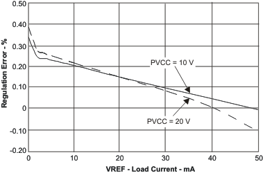
| VREF Load and Line Regulation | vs Load Current | Figure 1 |
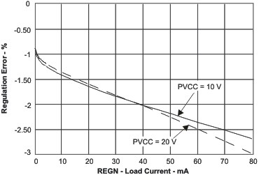
| REGN Load and Line Regulation | vs Load Current | Figure 2 |
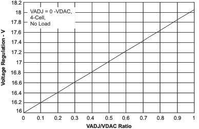
| BAT Voltage | vs VADJ/VDAC Ratio | Figure 3 |
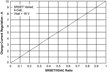
| Charge Current | vs SRSET/VDAC Ratio | Figure 4 |
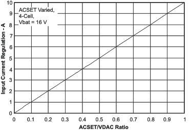
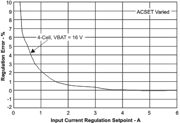
| Input Current | vs ACSET/VDAC Ratio | Figure 5 |
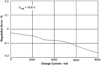
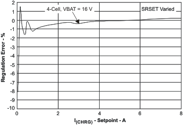
| BAT Voltage Regulation Accuracy | vs Charge Current | Figure 6 |
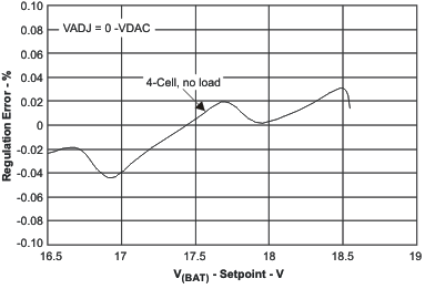
| BAT Voltage Regulation Accuracy | Figure 7 | |
| Charge Current Regulation Accuracy | Figure 8 | |
| Input Current Regulation (DPM) Accuracy | Figure 9 | |
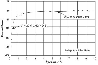
| VIADAPT Input Current Sense Amplifier Accuracy | Figure 10 | |
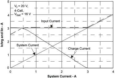
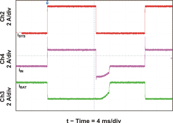
| Input Regulation Current (DPM), and Charge Current | vs System Current | Figure 11 |
| Transient System Load (DPM) Response | Figure 12 | |
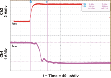
| Fast (DPM) Response | Figure 13 | |
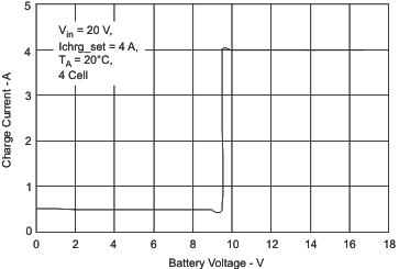
| Charge Current Regulation | vs BAT Voltage | Figure 14 |
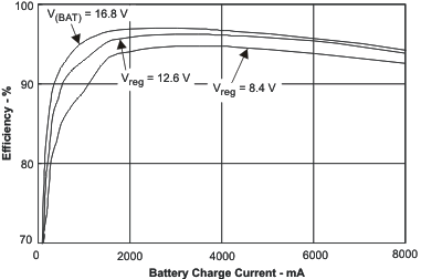
| Efficiency | vs Battery Charge Current | Figure 15 |
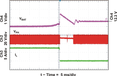
| Battery Removal (from Constant Current Mode) | Figure 16 | |
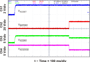
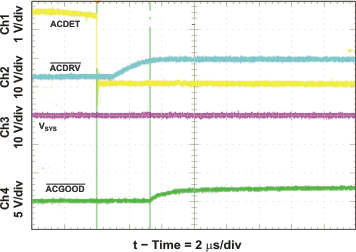
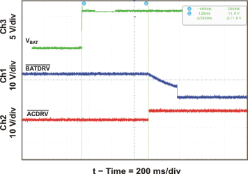
| ACDRV and BATDRV Startup | Figure 17 | |
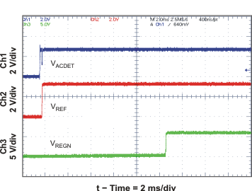
| REF and REGN Startup | Figure 18 | |
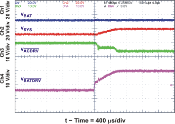
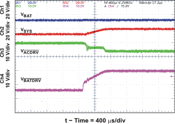
| System Selector on Adapter Insertion with 390-μF SYS-to-PGND System Capacitor | Figure 19 | |
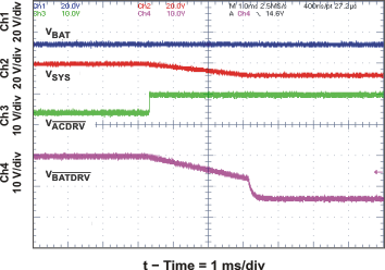
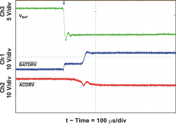
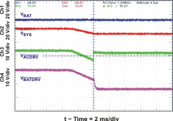
| System Selector on Adapter Removal with 390-μF SYS-to-PGND System Capacitor | Figure 20 | |
| System Selector LEARN Turn-On with 390-μF SYS-to-PGND System Capacitor | Figure 21 | |
| System Selector LEARN Turn-Off with 390-μF SYS-to-PGND System Capacitor | Figure 22 | |
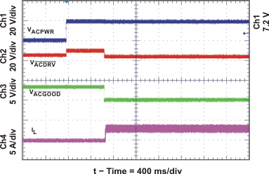
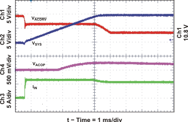
| System Selector on Adapter Insertion | Figure 23 | |
| Selector Gate Drive Voltages, 700 ms delay after ACDET | Figure 24 | |
| System Selector when Adapter Removed | Figure 25 | |
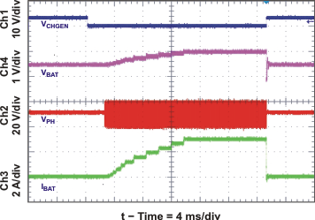
| Charge Enable / Disable and Current Soft-Start | Figure 26 | |
| Nonsynchronous to Synchronous Transition | Figure 27 | |
| Synchronous to Nonsynchronous Transition | Figure 28 | |
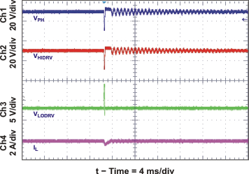
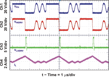
| Near 100% Duty Cycle Bootstrap Recharge Pulse | Figure 29 | |
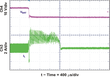
| Battery Shorted Charger Response, Over Current Protection (OCP) and Charge Current Regulation | Figure 30 | |
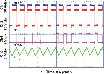
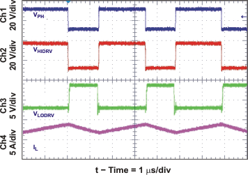
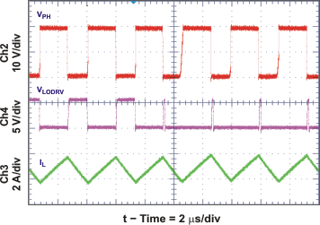
| Continuous Conduction Mode (CCM) Switching Waveforms | Figure 32 | |
| Discontinuous Conduction Mode (DCM) Switching Waveforms | Figure 31 | |
| BATSHORT Entry | Figure 33 | |
| BATSHORT Exit | Figure 34 | |
(1) Test results based on Figure 37 application schematic. VIN = 20 V, VBAT = 3-cell Li-Ion, ICHG = 3 A, IADAPTER_LIMIT = 4 A, TA = 25°C, unless otherwise specified.
