SLUSBH1C November 2013 – December 2014
PRODUCTION DATA.
- 1 Features
- 2 Applications
- 3 Description
- 4 Simplified Schematic
- 5 Revision History
- 6 Device Comparison Table
- 7 Pin Configuration and Functions
-
8 Specifications
- 8.1 Absolute Maximum Ratings
- 8.2 ESD Ratings
- 8.3 Recommended Operating Conditions
- 8.4 Thermal Information
- 8.5 Supply Current
- 8.6 Digital Input and Output DC Characteristics
- 8.7 LDO Regulator, Wake-up, and Auto-Shutdown DC Characteristics
- 8.8 LDO Regulator, Wake-up, and Auto-shutdown AC Characteristics
- 8.9 ADC (Temperature and Cell Measurement) Characteristics
- 8.10 Integrating ADC (Coulomb Counter) Characteristics
- 8.11 I2C-Compatible Interface Communication Timing Characteristics
- 8.12 SHUTDOWN and WAKE-UP Timing
- 8.13 Typical Characteristics
- 9 Detailed Description
- 10Application and Implementation
- 11Power Supply Recommendation
- 12Layout
- 13Device and Documentation Support
- 14Mechanical, Packaging, and Orderable Information
7 Pin Configuration and Functions
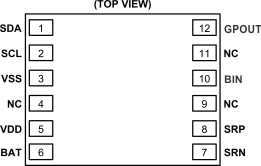
Pin Functions
| PIN | TYPE(1) | DESCRIPTION | |
|---|---|---|---|
| NAME | NUMBER | ||
| BAT | 6 | PI, AI | LDO regulator input and battery voltage measurement input. Kelvin sense connect to positive battery terminal (PACKP). Connect a capacitor (1 µF) between BAT and VSS. Place the capacitor close to the gauge. |
| BIN | 10 | DI | Battery insertion detection input. If OpConfig[BI_PU_EN] = 1 (default), a logic low on the pin is detected as battery insertion. For a removable pack, the BIN pin can be connected to VSS through a pulldown resistor on the pack, typically the 10-kΩ thermistor; the system board should use a 1.8-MΩ pullup resistor to VDD to ensure the BIN pin is high when a battery is removed. If the battery is embedded in the system, it is recommended to leave [BI_PU_EN] = 1 and use a 10-kΩ pulldown resistor from BIN to VSS. If [BI_PU_EN] = 0, then the host must inform the gauge of battery insertion and removal with the BAT_INSERT and BAT_REMOVE subcommands. A 10-kΩ pulldown resistor should be placed between BIN and VSS, even if this pin is unused. NOTE: The BIN pin must not be shorted directly to VCC or VSS and any pullup resistor on the BIN pin must be connected only to VDD and not an external voltage rail. |
| GPOUT | 12 | DO | This open-drain output can be configured to indicate BAT_LOW when the OpConfig[BATLOWEN] bit is set. By default [BATLOWEN] is cleared and this pin performs an interrupt function (SOC_INT) by pulsing for specific events, such as a change in state-of-charge. Signal polarity for these functions is controlled by the [GPIOPOL] configuration bit. This pin should not be left floating, even if unused; therefore, a 10-kΩ pullup resistor is recommended. If the device is in shutdown mode, then toggling GPOUT will make the gauge exit shutdown. Therefore, it is recommended to connect GPOUT to a GPIO of the host MCU. |
| NC | 4, 9, 11 | — | No internal connection. May be left floating or tied to VSS. |
| SCL | 2 | DIO | Slave I2C serial bus for communication with system (Master). Open-drain pins. Use with external 10-kΩ pullup resistors (typical) for each pin. If the external pullup resistors will be disconnected from these pins during normal operation, recommend using external 1-MΩ pulldown resistors to VSS at each pin to avoid floating inputs. |
| SDA | 1 | DIO | |
| SRN | 7 | AI | Coulomb counter differential inputs expecting an external 10 mΩ, 1% sense resistor in the high-side current path. Kelvin sense connect SRP to the positive battery terminal (PACKP) side of the external sense resistor. Kelvin sense connect SRN to the other side of the external sense resistor, the positive connection to the system (VSYS). See the Simplified Schematic. No calibration is required. The fuel gauge is pre-calibrated for a standard 10 mΩ, 1% sense resistor. |
| SRP | 8 | AI | |
| VDD | 5 | PO | 1.8-V regulator output. Decouple with 0.47-μF ceramic capacitor to VSS. This pin is not intended to provide power for other devices in the system. |
| VSS | 3 | PI | Ground pin |
(1) IO = Digital input-output, AI = Analog input, P = Power connection