SLUSBH1C November 2013 – December 2014
PRODUCTION DATA.
- 1 Features
- 2 Applications
- 3 Description
- 4 Simplified Schematic
- 5 Revision History
- 6 Device Comparison Table
- 7 Pin Configuration and Functions
-
8 Specifications
- 8.1 Absolute Maximum Ratings
- 8.2 ESD Ratings
- 8.3 Recommended Operating Conditions
- 8.4 Thermal Information
- 8.5 Supply Current
- 8.6 Digital Input and Output DC Characteristics
- 8.7 LDO Regulator, Wake-up, and Auto-Shutdown DC Characteristics
- 8.8 LDO Regulator, Wake-up, and Auto-shutdown AC Characteristics
- 8.9 ADC (Temperature and Cell Measurement) Characteristics
- 8.10 Integrating ADC (Coulomb Counter) Characteristics
- 8.11 I2C-Compatible Interface Communication Timing Characteristics
- 8.12 SHUTDOWN and WAKE-UP Timing
- 8.13 Typical Characteristics
- 9 Detailed Description
- 10Application and Implementation
- 11Power Supply Recommendation
- 12Layout
- 13Device and Documentation Support
- 14Mechanical, Packaging, and Orderable Information
8 Specifications
8.1 Absolute Maximum Ratings
over operating free-air temperature range (unless otherwise noted)(1)| MIN | MAX | UNIT | ||
|---|---|---|---|---|
| VBAT | BAT pin input voltage range | –0.3 | 6 | V |
| VSR | SRP and SRN pins input voltage range | –0.3 | VBAT + 0.3 | V |
| Differential voltage across SRP and SRN. ABS(SRP – SRN) | 2 | V | ||
| VDD | VDD pin supply voltage range (LDO output) | –0.3 | 2 | V |
| VIOD | Open-drain IO pins (SDA, SCL) | –0.3 | 6 | V |
| VIOPP | Push-pull IO pins (BIN) | –0.3 | VDD + 0.3 | V |
| TA | Operating free-air temperature range | –40 | 85 | °C |
| Storage temperature, Tstg | –65 | 150 | °C | |
(1) Stresses beyond those listed under "absolute maximum ratings" may cause permanent damage to the device. These are stress ratings only, and functional operation of the device at these or any other conditions beyond those indicated under "recommended operating conditions" is not implied. Exposure to absolute-maximum-rated conditions for extended periods may affect device reliability.
8.2 ESD Ratings
| VALUE | UNIT | |||
|---|---|---|---|---|
| V(ESD) | Electrostatic discharge | Human body model (HBM), per ANSI/ESDA/JEDEC JS-001(1) | ±1500 | V |
| Charged-device model (CDM), per JEDEC specification JESD22-C101(2) | ±250 | |||
(1) JEDEC document JEP155 states that 500-V HBM allows safe manufacturing with a standard ESD control process.
(2) JEDEC document JEP157 states that 250-V CDM allows safe manufacturing with a standard ESD control process.
8.3 Recommended Operating Conditions
TA = 30°C and VREGIN = VBAT = 3.6 V (unless otherwise noted)| MIN | TYP | MAX | UNIT | |||
|---|---|---|---|---|---|---|
| CBAT(1) | External input capacitor for internal LDO between BAT and VSS | Nominal capacitor values specified. Recommend a 5% ceramic X5R-type capacitor located close to the device. | 0.1 | μF | ||
| CLDO18(1) | External output capacitor for internal LDO between VDD and VSS | 0.47 | μF | |||
| VPU(1) | External pullup voltage for open-drain pins (SDA, SCL, GPOUT) | 1.62 | 3.6 | V | ||
(1) Specified by design. Not production tested.
8.4 Thermal Information
| THERMAL METRIC | DRZ (12 PINS) | UNIT | |
|---|---|---|---|
| RθJA | Junction-to-ambient thermal resistance | 64.1 | °C/W |
| RθJCtop | Junction-to-case (top) thermal resistance | 59.8 | |
| RθJB | Junction-to-board thermal resistance | 52.7 | |
| ψJT | Junction-to-top characterization parameter | 0.3 | |
| ψJB | Junction-to-board characterization parameter | 28.3 | |
| RθJCbot | Junction-to-case (bottom) thermal resistance | 2.4 | |
8.5 Supply Current
TA = 30°C and VREGIN = VBAT = 3.6V (unless otherwise noted)| PARAMETER | TEST CONDITIONS | MIN | TYP | MAX | UNIT | |
|---|---|---|---|---|---|---|
| ICC(1) | NORMAL mode current | ILOAD > Sleep Current(2) | 93 | μA | ||
| ISLP(1) | SLEEP mode current | ILOAD < Sleep Current(2) | 21 | μA | ||
| IHIB(1) | HIBERNATE mode current | ILOAD < Hibernate Current(2) | 9 | μA | ||
| ISD(1) | SHUTDOWN mode current | Fuel gauge in host commanded SHUTDOWN mode. (LDO regulator output disabled) |
0.6 | μA | ||
(1) Specified by design. Not production tested.
(2) Wake Comparator Disabled.
8.6 Digital Input and Output DC Characteristics
TA = –40°C to 85°C, typical values at TA = 30°C and VREGIN = 3.6 V (unless otherwise noted)| PARAMETER | TEST CONDITIONS | MIN | TYP | MAX | UNIT | |
|---|---|---|---|---|---|---|
| VIH(OD) | Input voltage, high(2) | External pullup resistor to VPU | VPU × 0.7 | V | ||
| VIH(PP) | Input voltage, high (3) | 1.4 | V | |||
| VIL | Input voltage, low(2)(3) | 0.6 | V | |||
| VOL | Output voltage, low(2) | 0.6 | V | |||
| IOH | Output source current, high(2) | 0.5 | mA | |||
| IOL(OD) | Output sink current, low(2) | –3 | mA | |||
| CIN(1) | Input capacitance(2)(3) | 5 | pF | |||
| Ilkg | Input leakage current (SCL, SDA, BIN) |
0.1 | μA | |||
| Input leakage current (GPOUT) | 1 | |||||
(1) Specified by design. Not production tested.
(2) Open Drain pins: (SCL, SDA, GPOUT)
(3) Push-Pull pin: (BIN)
8.7 LDO Regulator, Wake-up, and Auto-Shutdown DC Characteristics
TA = –40°C to 85°C, typical values at TA = 30°C and VREGIN = 3.6 V (unless otherwise noted)| PARAMETER | TEST CONDITIONS | MIN | TYP | MAX | UNIT | |
|---|---|---|---|---|---|---|
| VBAT | BAT pin regulator input | 2.45 | 4.5 | V | ||
| VDD | Regulator output voltage | 1.8 | V | |||
| UVLOIT+ | VBAT undervoltage lock-out LDO wake-up rising threshold |
2 | V | |||
| UVLOIT– | VBAT undervoltage lock-out LDO auto-shutdown falling threshold |
1.95 | V | |||
| VWU+(1) | GPOUT (input) LDO Wake-up rising edge threshold(2) | LDO Wake-up from SHUTDOWN mode | 1.2 | V | ||
(1) Specified by design. Not production tested.
(2) If the device is commanded to SHUTDOWN via I2C with VBAT > UVLOIT+, a wake-up rising edge trigger is required on GPOUT.
8.8 LDO Regulator, Wake-up, and Auto-shutdown AC Characteristics
TA = –40°C to 85°C, typical values at TA = 30°C and VREGIN = 3.6 V (unless otherwise noted)| PARAMETER | TEST CONDITIONS | MIN | TYP | MAX | UNIT | |
|---|---|---|---|---|---|---|
| tSHDN(1) | SHUTDOWN entry time | Time delay from SHUTDOWN command to LDO output disable. | 250 | ms | ||
| tSHUP(1) | SHUTDOWN GPOUT low time | Minimum low time of GPOUT (input) in SHUTDOWN before WAKEUP | 10 | μs | ||
| tVDD(1) | Initial VDD output delay | 13 | ms | |||
| tWUVDD(1) | Wake-up VDD output delay | Time delay from rising edge of GPOUT (input) to nominal VDD output. | 8 | ms | ||
| tPUCD | Power-up communication delay | Time delay from rising edge of REGIN to the Active state. Includes firmware initialization time. | 250 | ms | ||
(1) Specified by design. Not production tested.
8.9 ADC (Temperature and Cell Measurement) Characteristics
TA = –40°C to 85°C; typical values at TA = 30°C and VREGIN = 3.6 V (unless otherwise noted)| PARAMETER | TEST CONDITIONS | MIN | TYP | MAX | UNIT | |
|---|---|---|---|---|---|---|
| VIN(BAT) | BAT pin voltage measurement range | Voltage divider enabled | 2.45 | 4.5 | V | |
| tADC_CONV | Conversion time | 125 | ms | |||
| Effective resolution | 15 | bits | ||||
(1) Specified by design. Not tested in production.
8.10 Integrating ADC (Coulomb Counter) Characteristics
TA = –40°C to 85°C; typical values at TA = 30°C and VREGIN = 3.6 V (unless otherwise noted)| PARAMETER | TEST CONDITIONS | MIN | TYP | MAX | UNIT | |
|---|---|---|---|---|---|---|
| VSR | Input voltage range from BAT to SRX pins | BAT ± 25 | mV | |||
| tSR_CONV | Conversion time | Single conversion | 1 | s | ||
| Effective Resolution | Single conversion | 16 | bits | |||
(1) Specified by design. Not tested in production.
8.11 I2C-Compatible Interface Communication Timing Characteristics
TA = –40°C to 85°C; typical values at TA = 30°C and VREGIN = 3.6 V (unless otherwise noted)| MIN | TYP | MAX | UNIT | |||
|---|---|---|---|---|---|---|
| Standard Mode (100 kHz) | ||||||
| td(STA) | Start to first falling edge of SCL | 4 | μs | |||
| tw(L) | SCL pulse duration (low) | 4.7 | μs | |||
| tw(H) | SCL pulse duration (high) | 4 | μs | |||
| tsu(STA) | Setup for repeated start | 4.7 | μs | |||
| tsu(DAT) | Data setup time | Host drives SDA | 250 | ns | ||
| th(DAT) | Data hold time | Host drives SDA | 0 | ns | ||
| tsu(STOP) | Setup time for stop | 4 | μs | |||
| t(BUF) | Bus free time between stop and start | Includes Command Waiting Time | 66 | μs | ||
| tf | SCL or SDA fall time(1) | 300 | ns | |||
| tr | SCL or SDA rise time(1) | 300 | ns | |||
| fSCL | Clock frequency(2) | 100 | kHz | |||
| Fast Mode (400 kHz) | ||||||
| td(STA) | Start to first falling edge of SCL | 600 | ns | |||
| tw(L) | SCL pulse duration (low) | 1300 | ns | |||
| tw(H) | SCL pulse duration (high) | 600 | ns | |||
| tsu(STA) | Setup for repeated start | 600 | ns | |||
| tsu(DAT) | Data setup time | Host drives SDA | 100 | ns | ||
| th(DAT) | Data hold time | Host drives SDA | 0 | ns | ||
| tsu(STOP) | Setup time for stop | 600 | ns | |||
| t(BUF) | Bus free time between stop and start | Includes Command Waiting Time | 66 | μs | ||
| tf | SCL or SDA fall time(1) | 300 | ns | |||
| tr | SCL or SDA rise time(1) | 300 | ns | |||
| fSCL | Clock frequency(2) | 400 | kHz | |||
(1) Specified by design. Not production tested.
(2) If the clock frequency (fSCL) is > 100 kHz, use 1-byte write commands for proper operation. All other transactions types are supported at 400 kHz. (See I2C Interface and I2C Command Waiting Time.)
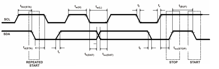 Figure 1. I2C-Compatible Interface Timing Diagrams
8.12 SHUTDOWN and WAKE-UP Timing
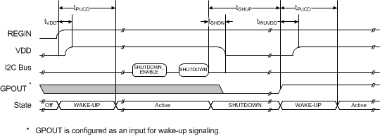 Figure 2. SHUTDOWN and WAKE-UP Timing Diagram
8.13 Typical Characteristics
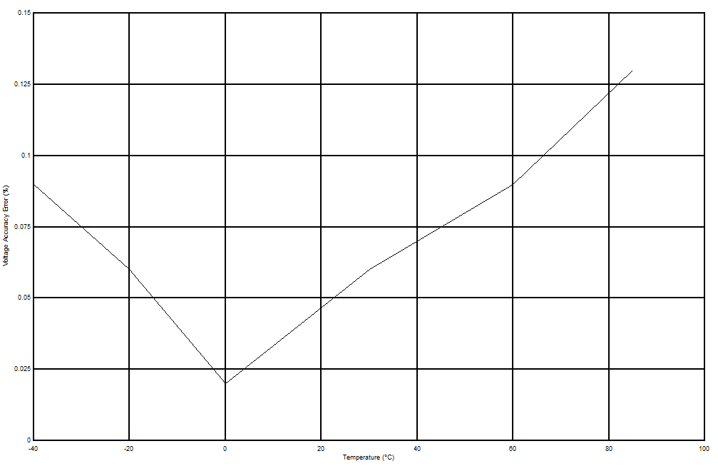 Figure 3. Voltage Accuracy
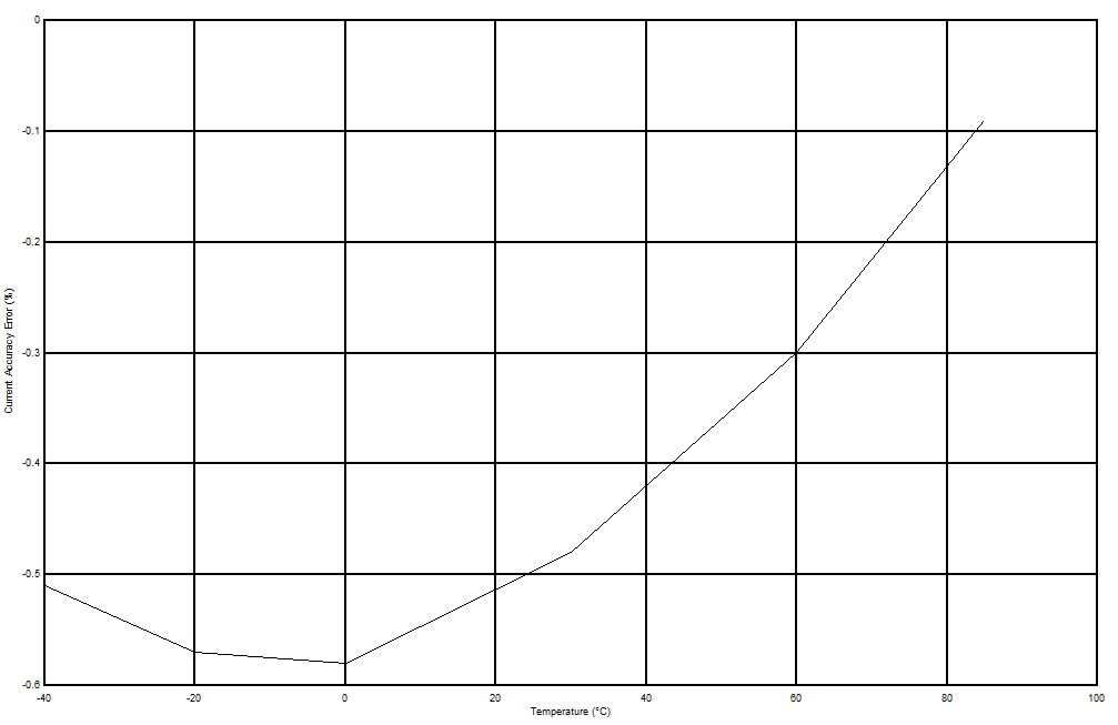 Figure 5. Current Accuracy
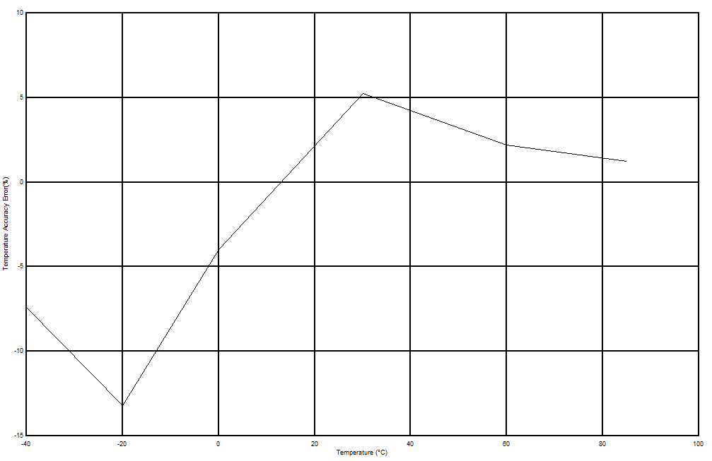 Figure 4. Temperature Accuracy