JAJSFE4B May 2015 – May 2018
PRODUCTION DATA.
- 1 特長
- 2 アプリケーション
- 3 概要
- 4 改訂履歴
- 5 Device Comparison Table
- 6 Pin Configuration and Functions
-
7 Specifications
- 7.1 Absolute Maximum Ratings
- 7.2 ESD Ratings
- 7.3 Recommended Operating Conditions
- 7.4 Thermal Information
- 7.5 Supply Current
- 7.6 Digital Input and Output DC Characteristics
- 7.7 Power-On Reset
- 7.8 2.5-V LDO Regulator
- 7.9 Internal Clock Oscillators
- 7.10 Integrating ADC (Coulomb Counter) Characteristics
- 7.11 ADC (Temperature and Cell Voltage) Characteristics
- 7.12 Data Flash Memory Characteristics
- 7.13 HDQ Communication Timing Characteristics
- 7.14 I2C-Compatible Interface Timing Characteristics
- 7.15 Typical Characteristics
-
8 Detailed Description
- 8.1 Overview
- 8.2 Functional Block Diagram
- 8.3
Feature Description
- 8.3.1 Fuel Gauging
- 8.3.2 Impedance Track Variables
- 8.3.3 Power Control
- 8.3.4 Autocalibration
- 8.3.5 Communications
- 8.4 Device Functional Modes
- 8.5 Programming
- 8.6 Register Maps
- 9 Application and Implementation
- 10Power Supply Recommendations
- 11Layout
- 12デバイスおよびドキュメントのサポート
- 13メカニカル、パッケージ、および注文情報
7.14 I2C-Compatible Interface Timing Characteristics
TA = –40°C to 85°C, CREG = 0.47 μF, 2.45 V < VREGIN = VBAT < 5.5 V; typical values at TA = 25°C and VREGIN = VBAT = 3.6 V (unless otherwise noted)| PARAMETER | TEST CONDITIONS | MIN | NOM | MAX | UNIT | |
|---|---|---|---|---|---|---|
| tr | SCL/SDA rise time | 300 | ns | |||
| tf | SCL/SDA fall time | 300 | ns | |||
| tw(H) | SCL pulse width (high) | 600 | ns | |||
| tw(L) | SCL pulse width (low) | 1.3 | μs | |||
| tsu(STA) | Setup for repeated start | 600 | ns | |||
| td(STA) | Start to first falling edge of SCL | 600 | ns | |||
| tsu(DAT) | Data setup time | 1000 | ns | |||
| th(DAT) | Data hold time | 0 | ns | |||
| tsu(STOP) | Setup time for stop | 600 | ns | |||
| tBUF | Bus free time between stop and start | 66 | μs | |||
| fSCL | Clock frequency (1) | 400 | kHz | |||
(1) If the clock frequency (fSCL) is > 100 kHz, use 1-byte write commands for proper operation. All other transactions types are supported at 400 kHz. (Refer to I2C Interface.)
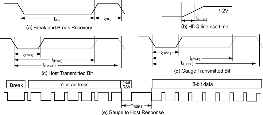
 Figure 1. HDQ Timing Diagrams
  Figure 2. I2C-Compatible Interface Timing Diagrams