JAJSDZ7B March 2016 – October 2017
PRODUCTION DATA.
- 1 特長
- 2 アプリケーション
- 3 概要
- 4 改訂履歴
- 5 Pin Configuration and Functions
-
6 Specifications
- 6.1 Absolute Maximum Ratings
- 6.2 ESD Ratings
- 6.3 Recommended Operating Conditions
- 6.4 Thermal Information
- 6.5 Electrical Characteristics: Supply Current
- 6.6 Electrical Characteristics: Power Supply Control
- 6.7 Electrical Characteristics: AFE Power-On Reset
- 6.8 Electrical Characteristics: AFE Watchdog Reset and Wake Timer
- 6.9 Electrical Characteristics: Current Wake Comparator
- 6.10 Electrical Characteristics: VC1, VC2, VC3, VC4, BAT, PACK
- 6.11 Electrical Characteristics: SMBD, SMBC
- 6.12 Electrical Characteristics: PRES, BTP_INT, DISP
- 6.13 Electrical Characteristics: LEDCNTLA, LEDCNTLB, LEDCNTLC
- 6.14 Electrical Characteristics: Coulomb Counter
- 6.15 Electrical Characteristics: CC Digital Filter
- 6.16 Electrical Characteristics: ADC
- 6.17 Electrical Characteristics: ADC Digital Filter
- 6.18 Electrical Characteristics: CHG, DSG FET Drive
- 6.19 Electrical Characteristics: PCHG FET Drive
- 6.20 Electrical Characteristics: FUSE Drive
- 6.21 Electrical Characteristics: Internal Temperature Sensor
- 6.22 Electrical Characteristics: TS1, TS2, TS3, TS4
- 6.23 Electrical Characteristics: PTC, PTCEN
- 6.24 Electrical Characteristics: Internal 1.8-V LDO
- 6.25 Electrical Characteristics: High-Frequency Oscillator
- 6.26 Electrical Characteristics: Low-Frequency Oscillator
- 6.27 Electrical Characteristics: Voltage Reference 1
- 6.28 Electrical Characteristics: Voltage Reference 2
- 6.29 Electrical Characteristics: Instruction Flash
- 6.30 Electrical Characteristics: Data Flash
- 6.31 Electrical Characteristics: OCD, SCC, SCD1, SCD2 Current Protection Thresholds
- 6.32 Timing Requirements: OCD, SCC, SCD1, SCD2 Current Protection Timing
- 6.33 Timing Requirements: SMBus
- 6.34 Timing Requirements: SMBus XL
- 6.35 Typical Characteristics
-
7 Detailed Description
- 7.1 Overview
- 7.2 Functional Block Diagram
- 7.3
Feature Description
- 7.3.1 Primary (1st Level) Safety Features
- 7.3.2 Secondary (2nd Level) Safety Features
- 7.3.3 Charge Control Features
- 7.3.4 Gas Gauging
- 7.3.5 Configuration
- 7.3.6 Battery Parameter Measurements
- 7.3.7 Battery Trip Point (BTP)
- 7.3.8 Lifetime Data Logging Features
- 7.3.9 Authentication
- 7.3.10 LED Display
- 7.3.11 Voltage
- 7.3.12 Current
- 7.3.13 Temperature
- 7.3.14 Communications
- 7.4 Device Functional Modes
- 8 Applications and Implementation
- 9 Power Supply Recommendations
- 10Layout
- 11デバイスおよびドキュメントのサポート
- 12メカニカル、パッケージ、および注文情報
パッケージ・オプション
メカニカル・データ(パッケージ|ピン)
- RSM|32
サーマルパッド・メカニカル・データ
- RSM|32
発注情報
6 Specifications
6.1 Absolute Maximum Ratings
Over-operating free-air temperature range (unless otherwise noted)(1)| MIN | MAX | UNIT | ||
|---|---|---|---|---|
| Supply voltage range, VCC | BAT, VCC, PBI | –0.3 | 30 | V |
| Input voltage range, VIN | PACK, SMBC, SMBD, PRES or SHUTDN, BTP_INT, DISP | –0.3 | 30 | V |
| TS1, TS2, TS3, TS4 | –0.3 | VREG + 0.3 | V | |
| PTC, PTCEN, LEDCNTLA, LEDCNTLB, LEDCNTLC | –0.3 | VBAT + 0.3 | V | |
| SRP, SRN | –0.3 | 0.3 | V | |
| VC4 | VC3 – 0.3 | VC3 + 8.5 V, or VSS + 30 | V | |
| VC3 | VC2 – 0.3 | VC2 + 8.5 V, or VSS + 30 | V | |
| VC2 | VC1 – 0.3 | VC1 + 8.5 V, or VSS + 30 | V | |
| VC1 | VSS – 0.3 | VSS + 8.5 V, or VSS + 30 V | V | |
| Output voltage range, VO | CHG, DSG | –0.3 | 32 | |
| PCHG, FUSE | –0.3 | 30 | V | |
| Maximum VSS current, ISS | 50 | mA | ||
| TSTG | Storage temperature | –65 | 150 | °C |
| Lead temperature (soldering, 10 s), TSOLDER | 300 | °C | ||
(1) Stresses beyond those listed under absolute maximum ratings may cause permanent damage to the device. These are stress ratings only, and functional operation of the device at these or any other conditions beyond those indicated under recommended operating conditions is not implied. Exposure to absolute–maximum–rated conditions for extended periods may affect device reliability.
6.2 ESD Ratings
| VALUE | UNIT | |||
|---|---|---|---|---|
| V(ESD) | Electrostatic discharge | Human-body model (HBM), per ANSI/ESDA/JEDEC JS-001(1) | ±2000 | V |
| Charged-device model (CDM), per JEDEC specification JESD22-C101(2) | ±500 | |||
(1) JEDEC document JEP155 states that 500-V HBM allows safe manufacturing with a standard ESD control process.
(2) JEDEC document JEP157 states that 250-V CDM allows safe manufacturing with a standard ESD control process.
6.3 Recommended Operating Conditions
Typical values stated where TA = 25°C and VCC = 14.4 V, Min/Max values stated where TA = –40°C to 85°C and VCC = 2.2 V to 26 V (unless otherwise noted)| MIN | NOM | MAX | UNIT | ||||
|---|---|---|---|---|---|---|---|
| VCC | Supply voltage | BAT, VCC, PBI | 2.2 | 26 | V | ||
| VSHUTDOWN– | Shutdown voltage | VPACK < VSHUTDOWN– | 1.8 | 2.0 | 2.2 | V | |
| VSHUTDOWN+ | Start-up voltage | VPACK > VSHUTDOWN– + VHYS | 2.05 | 2.25 | 2.45 | V | |
| VHYS | Shutdown voltage hysteresis | VSHUTDOWN+ – VSHUTDOWN– | 250 | mV | |||
| VIN | Input voltage range | PACK, SMBC, SMBD, PRES, BTP_IN, DISP | 26 | V | |||
| TS1, TS2, TS3, TS4 | VREG | ||||||
| PTC, PTCEN, LEDCNTLA, LEDCNTLB, LEDCNTLC | VBAT | ||||||
| SRP, SRN | –0.2 | 0.2 | |||||
| VC4 | VVC3 | VVC3 + 5 | |||||
| VC3 | VVC2 | VVC2 + 5 | |||||
| VC2 | VVC1 | VVC1 + 5 | |||||
| VC1 | VVSS | VVSS + 5 | |||||
| VO | Output voltage range | CHG, DSG, PCHG, FUSE | 26 | V | |||
| CPBI | External PBI capacitor | 2.2 | µF | ||||
| TOPR | Operating temperature | –40 | 85 | °C | |||
6.4 Thermal Information
| THERMAL METRIC(1) | bq4050 | UNIT | ||
|---|---|---|---|---|
| RSM (QFN) | ||||
| 32 PINS | ||||
| RθJA, High K | Junction-to-ambient thermal resistance | 47.4 | °C/W | |
| RθJC(top) | Junction-to-case(top) thermal resistance | 40.3 | °C/W | |
| RθJB | Junction-to-board thermal resistance | 14.7 | °C/W | |
| ψJT | Junction-to-top characterization parameter | 0.8 | °C/W | |
| ψJB | Junction-to-board characterization parameter | 14.4 | °C/W | |
| RθJC(bottom) | Junction-to-case(bottom) thermal resistance | 3.8 | °C/W | |
(1) For more information about traditional and new thermal metrics, see the Semiconductor and IC Package Thermal Metrics application report, SPRA953.
6.5 Electrical Characteristics: Supply Current
Typical values stated where TA = 25°C and VCC = 14.4 V, Min/Max values stated where TA = –40°C to 85°C and VCC = 2.2 V to 20 V (unless otherwise noted)| PARAMETER | TEST CONDITIONS | MIN | TYP | MAX | UNIT | ||
|---|---|---|---|---|---|---|---|
| INORMAL | NORMAL mode | CHG on. DSG on, no Flash write | 336 | µA | |||
| ISLEEP | SLEEP mode | CHG off, DSG on, no SBS communication | 75 | µA | |||
| CHG off, DSG off, no SBS communication | 52 | ||||||
| ISHUTDOWN | SHUTDOWN mode | 1.6 | µA | ||||
6.6 Electrical Characteristics: Power Supply Control
Typical values stated where TA = 25°C and VCC = 14.4 V, Min/Max values stated where TA = –40°C to 85°C and VCC = 2.2 V to 26 V (unless otherwise noted)| PARAMETER | TEST CONDITIONS | MIN | TYP | MAX | UNIT | |
|---|---|---|---|---|---|---|
| VSWITCHOVER– | BAT to VCC switchover voltage | VBAT < VSWITCHOVER– | 1.95 | 2.1 | 2.2 | V |
| VSWITCHOVER+ | VCC to BAT switchover voltage | VBAT > VSWITCHOVER– + VHYS | 2.9 | 3.1 | 3.25 | V |
| VHYS | Switchover voltage hysteresis | VSWITCHOVER+ – VSWITCHOVER– | 1000 | mV | ||
| ILKG | Input Leakage current | BAT pin, BAT = 0 V, VCC = 25 V, PACK = 25 V | 1 | µA | ||
| PACK pin, BAT = 25 V, VCC = 0 V, PACK = 0 V | 1 | |||||
| BAT and PACK terminals, BAT = 0 V, VCC = 0 V, PACK = 0 V, PBI = 25 V | 1 | |||||
| RPD | Internal pulldown resistance | PACK | 30 | 40 | 50 | kΩ |
6.7 Electrical Characteristics: AFE Power-On Reset
Typical values stated where TA = 25°C and VCC = 14.4 V, Min/Max values stated where TA = –40°C to 85°C and VCC = 2.2 V to 26 V (unless otherwise noted)| PARAMETER | TEST CONDITIONS | MIN | TYP | MAX | UNIT | |
|---|---|---|---|---|---|---|
| VREGIT– | Negative-going voltage input | VREG | 1.51 | 1.55 | 1.59 | V |
| VHYS | Power-on reset hysteresis | VREGIT+ – VREGIT– | 70 | 100 | 130 | mV |
| tRST | Power-on reset time | 200 | 300 | 400 | µs | |
6.8 Electrical Characteristics: AFE Watchdog Reset and Wake Timer
Typical values stated where TA = 25°C and VCC = 14.4 V, Min/Max values stated where TA = –40°C to 85°C and VCC = 2.2 V to 26 V (unless otherwise noted)| PARAMETER | TEST CONDITIONS | MIN | TYP | MAX | UNIT | |
|---|---|---|---|---|---|---|
| tWDT | AFE watchdog timeout | tWDT = 500 | 372 | 500 | 628 | ms |
| tWDT = 1000 | 744 | 1000 | 1256 | |||
| tWDT = 2000 | 1488 | 2000 | 2512 | |||
| tWDT = 4000 | 2976 | 4000 | 5024 | |||
| tWAKE | AFE wake timer | tWAKE = 250 | 186 | 250 | 314 | ms |
| tWAKE = 500 | 372 | 500 | 628 | |||
| tWAKE = 1000 | 744 | 1000 | 1256 | |||
| tWAKE = 512 | 1488 | 2000 | 2512 | |||
| tFETOFF | FET off delay after reset | tFETOFF = 512 | 409 | 512 | 614 | ms |
6.9 Electrical Characteristics: Current Wake Comparator
Typical values stated where TA = 25°C and VCC = 14.4 V, Min/Max values stated where TA = –40°C to 85°C and VCC = 2.2 V to 26 V (unless otherwise noted)| PARAMETER | TEST CONDITIONS | MIN | TYP | MAX | UNIT | |
|---|---|---|---|---|---|---|
| VWAKE | Wake voltage threshold | VWAKE = ±0.625 mV | ±0.3 | ±0.625 | ±0.9 | mV |
| VWAKE = ±1.25 mV | ±0.6 | ±1.25 | ±1.8 | |||
| VWAKE = ±2.5 mV | ±1.2 | ±2.5 | ±3.6 | |||
| VWAKE = ±5 mV | ±2.4 | ±5.0 | ±7.2 | |||
| VWAKE(DRIFT) | Temperature drift of VWAKE accuracy | 0.5% | °C | |||
| tWAKE | Time from application of current to wake interrupt | 700 | µs | |||
| tWAKE(SU) | Wake comparator startup time | 500 | 1000 | µs | ||
6.10 Electrical Characteristics: VC1, VC2, VC3, VC4, BAT, PACK
Typical values stated where TA = 25°C and VCC = 14.4 V, Min/Max values stated where TA = –40°C to 85°C and VCC = 2.2 V to 26 V (unless otherwise noted)| PARAMETER | TEST CONDITIONS | MIN | TYP | MAX | UNIT | |
|---|---|---|---|---|---|---|
| K | Scaling factor | VC1–VSS, VC2–VC1, VC3–VC2, VC4–VC3 | 0.1980 | 0.2000 | 0.2020 | — |
| BAT–VSS, PACK–VSS | 0.049 | 0.050 | 0.051 | |||
| VREF2 | 0.490 | 0.500 | 0.510 | |||
| VIN | Input voltage range | VC1–VSS, VC2–VC1, VC3–VC2, VC4–VC3 | –0.2 | 5 | V | |
| BAT–VSS, PACK–VSS | –0.2 | 20 | ||||
| ILKG | Input leakage current | VC1, VC2, VC3, VC4, cell balancing off, cell detach detection off, ADC multiplexer off | 1 | µA | ||
| RCB | Internal cell balance resistance | RDS(ON) for internal FET switch at 2 V < VDS < 4 V | 200 | Ω | ||
| ICD | Internal cell detach check current | VCx > VSS + 0.8 V | 30 | 50 | 70 | µA |
6.11 Electrical Characteristics: SMBD, SMBC
Typical values stated where TA = 25°C and VCC = 14.4 V, Min/Max values stated where TA = –40°C to 85°C and VCC = 2.2 V to 26 V (unless otherwise noted)| PARAMETER | TEST CONDITIONS | MIN | TYP | MAX | UNIT | ||
|---|---|---|---|---|---|---|---|
| VIH | Input voltage high | SMBC, SMBD, VREG = 1.8 V | 1.3 | V | |||
| VIL | Input voltage low | SMBC, SMBD, VREG = 1.8 V | 0.8 | V | |||
| VOL | Output low voltage | SMBC, SMBD, VREG = 1.8 V, IOL = 1.5 mA | 0.4 | V | |||
| CIN | Input capacitance | 5 | pF | ||||
| ILKG | Input leakage current | 1 | µA | ||||
| RPD | Pulldown resistance | 0.7 | 1.0 | 1.3 | MΩ | ||
6.12 Electrical Characteristics: PRES, BTP_INT, DISP
Typical values stated where TA = 25°C and VCC = 14.4 V, Min/Max values stated where TA = –40°C to 85°C and VCC = 2.2 V to 26 V (unless otherwise noted)| PARAMETER | TEST CONDITIONS | MIN | TYP | MAX | UNIT | |
|---|---|---|---|---|---|---|
| VIH | High-level input | 1.3 | V | |||
| VIL | Low-level input | 0.55 | V | |||
| VOH | Output voltage high | VBAT > 5.5 V, IOH = –0 µA | 3.5 | V | ||
| VBAT > 5.5 V, IOH = –10 µA | 1.8 | |||||
| VOL | Output voltage low | IOL = 1.5 mA | 0.4 | V | ||
| CIN | Input capacitance | 5 | pF | |||
| ILKG | Input leakage current | 1 | µA | |||
| RO | Output reverse resistance | Between PRES or BTP_INT or DISP and PBI | 8 | kΩ | ||
6.13 Electrical Characteristics: LEDCNTLA, LEDCNTLB, LEDCNTLC
Typical values stated where TA = 25°C and VCC = 14.4 V, Min/Max values stated where TA = –40°C to 85°C and VCC = 2.2 V to 26 V (unless otherwise noted)| PARAMETER | TEST CONDITIONS | MIN | TYP | MAX | UNIT | |
|---|---|---|---|---|---|---|
| VIH | High-level input | 1.45 | V | |||
| VIL | Low-level input | 0.55 | V | |||
| VOH | Output voltage high | VBAT > 3.0 V, IOH = –22.5 mA | VBAT – 1.6 | V | ||
| VOL | Output voltage low | IOL = 1.5 mA | 0.4 | V | ||
| ISC | High level output current protection | –30 | –45 | –6 0 | mA | |
| IOL | Low level output current | VBAT > 3.0 V, VOH = 0.4 V | 15.75 | 22.5 | 29.25 | mA |
| ILEDCNTLx | Current matching between LEDCNTLx | VBAT = VLEDCNTLx + 2.5 V | ±1% | |||
| CIN | Input capacitance | 20 | pF | |||
| ILKG | Input leakage current | 1 | µA | |||
| fLEDCNTLx | Frequency of LED pattern | 124 | Hz | |||
6.14 Electrical Characteristics: Coulomb Counter
Typical values stated where TA = 25°C and VCC = 14.4 V, Min/Max values stated where TA = –40°C to 85°C and VCC = 2.2 V to 26 V (unless otherwise noted)| PARAMETER | TEST CONDITIONS | MIN | TYP | MAX | UNIT |
|---|---|---|---|---|---|
| Input voltage range | –0.1 | 0.1 | V | ||
| Full scale range | –VREF1/10 | VREF1/10 | V | ||
| Integral nonlinearity(1) | 16-bit, best fit over input voltage range | ±5.2 | ±22.3 | LSB | |
| Offset error | 16-bit, Post-calibration | ±5 | ±10 | µV | |
| Offset error drift | 15-bit + sign, Post-calibration | 0.2 | 0.3 | µV/°C | |
| Gain error | 15-bit + sign, over input voltage range | ±0.2% | ±0.8% | FSR | |
| Gain error drift | 15-bit + sign, over input voltage range | 150 | PPM/°C | ||
| Effective input resistance | 2.5 | MΩ |
(1) 1 LSB = VREF1/(10 × 2N) = 1.215/(10 × 215) = 3.71 µV
6.15 Electrical Characteristics: CC Digital Filter
Typical values stated where TA = 25°C and VCC = 14.4 V, Min/Max values stated where TA = –40°C to 85°C and VCC = 2.2 V to 26 V (unless otherwise noted)| PARAMETER | TEST CONDITIONS | MIN | TYP | MAX | UNIT |
|---|---|---|---|---|---|
| Conversion time | Single conversion | 250 | ms | ||
| Effective resolution | Single conversion | 15 | Bits |
6.16 Electrical Characteristics: ADC
Typical values stated where TA = 25°C and VCC = 14.4 V, Min/Max values stated where TA = –40°C to 85°C and VCC = 2.2 V to 26 V (unless otherwise noted)| PARAMETER | TEST CONDITIONS | MIN | TYP | MAX | UNIT |
|---|---|---|---|---|---|
| Input voltage range | Internal reference (VREF1) | –0.2 | 1 | V | |
| External reference (VREG) | –0.2 | 0.8 × VREG | |||
| Full scale range | VFS = VREF1 or VREG | –VFS | VFS | V | |
| Integral nonlinearity(1) | 16-bit, best fit, –0.1 V to 0.8 × VREF1 | ±6.6 | LSB | ||
| 16-bit, best fit, –0.2 V to –0.1 V | ±13.1 | ||||
| Offset error(2) | 16-bit, Post-calibration, VFS = VREF1 | ±67 | ±157 | µV | |
| Offset error drift | 16-bit, Post-calibration, VFS = VREF1 | 0.6 | 3 | µV/°C | |
| Gain error | 16-bit, –0.1 V to 0.8 × VFS | ±0.2% | ±0.8% | FSR | |
| Gain error drift | 16-bit, –0.1 V to 0.8 × VFS | 150 | PPM/°C | ||
| Effective input resistance | 8 | MΩ |
(1) 1 LSB = VREF1/(2N) = 1.225/(215) = 37.4 µV (when tCONV = 31.25 ms)
(2) For VC1–VSS, VC2–VC1, VC3–VC2, VC4–VC3, VC4–VSS, PACK–VSS, and VREF1/2, the offset error is multiplied by (1/ADC multiplexer scaling factor (K)).
6.17 Electrical Characteristics: ADC Digital Filter
Typical values stated where TA = 25°C and VCC = 14.4 V, Min/Max values stated where TA = –40°C to 85°C and VCC = 2.2 V to 26 V (unless otherwise noted)| PARAMETER | TEST CONDITIONS | MIN | TYP | MAX | UNIT |
|---|---|---|---|---|---|
| Conversion time | Single conversion | 31.25 | ms | ||
| Single conversion | 15.63 | ||||
| Single conversion | 7.81 | ||||
| Single conversion | 1.95 | ||||
| Resolution | No missing codes | 16 | Bits | ||
| Effective resolution | With sign, tCONV = 31.25 ms | 14 | 15 | Bits | |
| With sign, tCONV = 15.63 ms | 13 | 14 | |||
| With sign, tCONV = 7.81 ms | 11 | 12 | |||
| With sign, tCONV = 1.95 ms | 9 | 10 |
6.18 Electrical Characteristics: CHG, DSG FET Drive
Typical values stated where TA = 25°C and VCC = 14.4 V, Min/Max values stated where TA = –40°C to 85°C and VCC = 2.2 V to 26 V (unless otherwise noted)| PARAMETER | TEST CONDITIONS | MIN | TYP | MAX | UNIT | ||
|---|---|---|---|---|---|---|---|
| Output voltage ratio | RatioDSG = (VDSG – VBAT)/VBAT, 2.2 V < VBAT < 4.92 V, 10 MΩ between PACK and DSG | 2.133 | 2.333 | 2.433 | — | ||
| RatioCHG = (VCHG – VBAT)/VBAT, 2.2 V < VBAT < 4.92 V, 10 MΩ between BAT and CHG | 2.133 | 2.333 | 2.433 | ||||
| V(FETON) | Output voltage, CHG and DSG on | VDSG(ON) = VDSG – VBAT, 4.92 V ≤ VBAT ≤ 18 V, 10 MΩ between PACK and DSG | 10.5 | 11.5 | 12 | V | |
| VCHG(ON) = VCHG – VBAT, 4.92 V ≤ VBAT ≤ 18 V, 10 MΩ between BAT and CHG | 10.5 | 11.5 | 12 | ||||
| V(FETOFF) | Output voltage, CHG and DSG off | VDSG(OFF) = VDSG – VPACK, 10 MΩ between PACK and DSG | –0.4 | 0.4 | V | ||
| VCHG(OFF) = VCHG – VBAT, 10 MΩ between BAT and CHG | –0.4 | 0.4 | |||||
| tR | Rise time | VDSG from 0% to 35% VDSG(ON)(TYP), VBAT ≥ 2.2 V, CL = 4.7 nF between DSG and PACK, 5.1 kΩ between DSG and CL, 10 MΩ between PACK and DSG | 200 | 500 | µs | ||
| VCHG from 0% to 35% VCHG(ON)(TYP), VBAT ≥ 2.2 V, CL = 4.7 nF between CHG and BAT, 5.1 kΩ between CHG and CL, 10 MΩ between BAT and CHG | 200 | 500 | |||||
| tF | Fall time | VDSG from VDSG(ON)(TYP) to 1 V, VBAT ≥ 2.2 V, CL = 4.7 nF between DSG and PACK, 5.1 kΩ between DSG and CL, 10 MΩ between PACK and DSG | 40 | 300 | µs | ||
| VCHG from VCHG(ON)(TYP) to 1 V, VBAT ≥ 2.2 V, CL = 4.7 nF between CHG and BAT, 5.1 kΩ between CHG and CL, 10 MΩ between BAT and CHG | 40 | 200 | |||||
6.19 Electrical Characteristics: PCHG FET Drive
Typical values stated where TA = 25°C and VCC = 14.4 V, Min/Max values stated where TA = –40°C to 85°C and VCC = 2.2 V to 26 V (unless otherwise noted)| PARAMETER | TEST CONDITIONS | MIN | TYP | MAX | UNIT | ||
|---|---|---|---|---|---|---|---|
| V(FETON) | Output voltage, PCHG on | VPCHG(ON) = VVCC – VPCHG, 10 MΩ between VCC and PCHG | 6 | 7 | 8 | V | |
| V(FETOFF) | Output voltage, PCHG off | VPCHG(OFF) = VVCC – VPCHG, 10 MΩ between VCC and PCHG | –0.4 | 0.4 | V | ||
| tR | Rise time | VPCHG from 10% to 90% VPCHG(ON)(TYP), VVCC ≥ 8 V, CL = 4.7 nF between PCHG and VCC, 5.1 kΩ between PCHG and CL, 10 MΩ between VCC and CHG | 40 | 200 | µs | ||
| tF | Fall time | VPCHG from 90% to 10% VPCHG(ON)(TYP), VCC ≥ 8 V, CL = 4.7 nF between PCHG and VCC, 5.1 kΩ between PCHG and CL, 10 MΩ between VCC and CHG | 40 | 200 | µs | ||
6.20 Electrical Characteristics: FUSE Drive
Typical values stated where TA = 25°C and VCC = 14.4 V, Min/Max values stated where TA = –40°C to 85°C and VCC = 2.2 V to 26 V (unless otherwise noted)| PARAMETER | TEST CONDITIONS | MIN | TYP | MAX | UNIT | ||
|---|---|---|---|---|---|---|---|
| VOH | Output voltage high | VBAT ≥ 8 V, CL = 1 nF, IAFEFUSE = 0 µA | 6 | 7 | 8.65 | V | |
| VBAT < 8 V, CL = 1 nF, IAFEFUSE = 0 µA | VBAT – 0.1 | VBAT | |||||
| VIH | High-level input | 1.5 | 2.0 | 2.5 | V | ||
| IAFEFUSE(PU) | Internal pullup current | VBAT ≥ 8 V, VAFEFUSE = VSS | 150 | 330 | nA | ||
| RAFEFUSE | Output impedance | 2 | 2.6 | 3.2 | kΩ | ||
| CIN | Input capacitance | 5 | pF | ||||
| tDELAY | Fuse trip detection delay | 128 | 256 | µs | |||
| tRISE | Fuse output rise time | VBAT ≥ 8 V, CL = 1 nF, VOH = 0 V to 5 V | 5 | 20 | µs | ||
6.21 Electrical Characteristics: Internal Temperature Sensor
Typical values stated where TA = 25°C and VCC = 14.4 V, Min/Max values stated where TA = –40°C to 85°C and VCC = 2.2 V to 26 V (unless otherwise noted)| PARAMETER | TEST CONDITIONS | MIN | TYP | MAX | UNIT | |
|---|---|---|---|---|---|---|
| VTEMP | Internal temperature sensor voltage drift | VTEMPP | –1.9 | –2.0 | –2.1 | mV/°C |
| VTEMPP – VTEMPN, assured by design | 0.177 | 0.178 | 0.179 | |||
6.22 Electrical Characteristics: TS1, TS2, TS3, TS4
Typical values stated where TA = 25°C and VCC = 14.4 V, Min/Max values stated where TA = –40°C to 85°C and VCC = 2.2 V to 26 V (unless otherwise noted)| PARAMETER | TEST CONDITIONS | MIN | TYP | MAX | UNIT | |
|---|---|---|---|---|---|---|
| VIN | Input voltage range | TS1, TS2, TS3, TS4, VBIAS = VREF1 | –0.2 | 0.8 × VREF1 | V | |
| TS1, TS2, TS3, TS4, VBIAS = VREG | –0.2 | 0.8 × VREG | ||||
| RNTC(PU) | Internal pullup resistance | TS1, TS2, TS3, TS4 | 14.4 | 18 | 21.6 | kΩ |
| RNTC(DRIFT) | Resistance drift over temperature | TS1, TS2, TS3, TS4 | –360 | –280 | –200 | PPM/°C |
6.23 Electrical Characteristics: PTC, PTCEN
Typical values stated where TA = 25°C and VCC = 14.4 V, Min/Max values stated where TA = –40°C to 85°C and VCC = 2.2 V to 26 V (unless otherwise noted)| PARAMETER | TEST CONDITIONS | MIN | TYP | MAX | UNIT | |
|---|---|---|---|---|---|---|
| RPTC(TRIP) | PTC trip resistance | 1.2 | 2.5 | 3.95 | MΩ | |
| VPTC(TRIP) | PTC trip voltage | VPTC(TRIP) = VPTCEN – VPTC | 200 | 500 | 890 | mV |
| IPTC | Internal PTC current bias | TA = –40°C to 110°C | 200 | 290 | 350 | nA |
| tPTC(DELAY) | PTC delay time | TA = –40°C to 110°C | 40 | 80 | 145 | ms |
6.24 Electrical Characteristics: Internal 1.8-V LDO
Typical values stated where TA = 25°C and VCC = 14.4 V, Min/Max values stated where TA = –40°C to 85°C and VCC = 2.2 V to 26 V (unless otherwise noted)| PARAMETER | TEST CONDITIONS | MIN | TYP | MAX | UNIT | ||
|---|---|---|---|---|---|---|---|
| VREG | Regulator voltage | 1.6 | 1.8 | 2.0 | V | ||
| ΔVO(TEMP) | Regulator output over temperature | ΔVREG/ΔTA, IREG = 10 mA | ±0.25% | ||||
| ΔVO(LINE) | Line regulation | ΔVREG/ΔVBAT, VBAT = 10 mA | –0 .6% | 0.5% | |||
| ΔVO(LOAD) | Load regulation | ΔVREG/ΔIREG, IREG = 0 mA to 10 mA | –1.5% | 1.5% | |||
| IREG | Regulator output current limit | VREG = 0.9 × VREG(NOM), VIN > 2.2 V | 20 | mA | |||
| ISC | Regulator short-circuit current limit | VREG = 0 × VREG(NOM) | 25 | 40 | 55 | mA | |
| PSRRREG | Power supply rejection ratio | ΔVBAT/ΔVREG, IREG = 10 mA ,VIN > 2.5 V, f = 10 Hz | 40 | dB | |||
| VSLEW | Slew rate enhancement voltage threshold | VREG | 1.58 | 1.65 | V | ||
6.25 Electrical Characteristics: High-Frequency Oscillator
Typical values stated where TA = 25°C and VCC = 14.4 V, Min/Max values stated where TA = –40°C to 85°C and VCC = 2.2 V to 26 V (unless otherwise noted)| PARAMETER | TEST CONDITIONS | MIN | TYP | MAX | UNIT | |
|---|---|---|---|---|---|---|
| fHFO | Operating frequency | 16.78 | MHz | |||
| fHFO(ERR) | Frequency error | TA = –20°C to 70°C, includes frequency drift | –2.5% | ±0.25% | 2.5% | |
| TA = –40°C to 85°C, includes frequency drift | –3.5% | ±0.25% | 3.5% | |||
| tHFO(SU) | Start-up time | TA = –20°C to 85°C, oscillator frequency within +/–3% of nominal | 4 | ms | ||
| oscillator frequency within +/–3% of nominal | 100 | µs | ||||
6.26 Electrical Characteristics: Low-Frequency Oscillator
Typical values stated where TA = 25°C and VCC = 14.4 V, Min/Max values stated where TA = –40°C to 85°C and VCC = 2.2 V to 26 V (unless otherwise noted)| PARAMETER | TEST CONDITIONS | MIN | TYP | MAX | UNIT | |
|---|---|---|---|---|---|---|
| fLFO | Operating frequency | 262.144 | kHz | |||
| fLFO(ERR) | Frequency error | TA = –20°C to 70°C, includes frequency drift | –1.5% | ±0.25% | 1.5% | |
| TA = –40°C to 85°C, includes frequency drift | –2.5 | ±0.25 | 2.5 | |||
| fLFO(FAIL) | Failure detection frequency | 30 | 80 | 100 | kHz | |
6.27 Electrical Characteristics: Voltage Reference 1
Typical values stated where TA = 25°C and VCC = 14.4 V, Min/Max values stated where TA = –40°C to 85°C and VCC = 2.2 V to 26 V (unless otherwise noted)| PARAMETER | TEST CONDITIONS | MIN | TYP | MAX | UNIT | |
|---|---|---|---|---|---|---|
| VREF1 | Internal reference voltage | TA = 25°C, after trim | 1.21 | 1.215 | 1.22 | V |
| VREF1(DRIFT) | Internal reference voltage drift | TA = 0°C to 60°C, after trim | ±50 | PPM/°C | ||
| TA = –40°C to 85°C, after trim | ±80 | |||||
6.28 Electrical Characteristics: Voltage Reference 2
Typical values stated where TA = 25°C and VCC = 14.4 V, Min/Max values stated where TA = –40°C to 85°C and VCC = 2.2 V to 26 V (unless otherwise noted)| PARAMETER | TEST CONDITIONS | MIN | TYP | MAX | UNIT | |
|---|---|---|---|---|---|---|
| VREF2 | Internal reference voltage | TA = 25°C, after trim | 1.22 | 1.225 | 1.23 | V |
| VREF2(DRIFT) | Internal reference voltage drift | TA = 0°C to 60°C, after trim | ±50 | PPM/°C | ||
| TA = –40°C to 85°C, after trim | ±80 | |||||
6.29 Electrical Characteristics: Instruction Flash
Typical values stated where TA = 25°C and VCC = 14.4 V, Min/Max values stated where TA = –40°C to 85°C and VCC = 2.2 V to 26 V (unless otherwise noted)| PARAMETER | TEST CONDITIONS | MIN | TYP | MAX | UNIT | |
|---|---|---|---|---|---|---|
| Data retention | 10 | Years | ||||
| Flash programming write cycles | 1000 | Cycles | ||||
| tPROGWORD | Word programming time | TA = –40°C to 85°C | 40 | µs | ||
| tMASSERASE | Mass-erase time | TA = –40°C to 85°C | 40 | ms | ||
| tPAGEERASE | Page-erase time | TA = –40°C to 85°C | 40 | ms | ||
| IFLASHREAD | Flash-read current | TA = –40°C to 85°C | 2 | mA | ||
| IFLASHWRITE | Flash-write current | TA = –40°C to 85°C | 5 | mA | ||
| IFLASHERASE | Flash-erase current | TA = –40°C to 85°C | 15 | mA | ||
6.30 Electrical Characteristics: Data Flash
Typical values stated where TA = 25°C and VCC = 14.4 V, Min/Max values stated where TA = –40°C to 85°C and VCC = 2.2 V to 26 V (unless otherwise noted)| PARAMETER | TEST CONDITIONS | MIN | TYP | MAX | UNIT | |
|---|---|---|---|---|---|---|
| Data retention | 10 | Years | ||||
| Flash programming write cycles | 20000 | Cycles | ||||
| tPROGWORD | Word programming time | TA = –40°C to 85°C | 40 | µs | ||
| tMASSERASE | Mass-erase time | TA = –40°C to 85°C | 40 | ms | ||
| tPAGEERASE | Page-erase time | TA = –40°C to 85°C | 40 | ms | ||
| IFLASHREAD | Flash-read current | TA = –40°C to 85°C | 1 | mA | ||
| IFLASHWRITE | Flash-write current | TA = –40°C to 85°C | 5 | mA | ||
| IFLASHERASE | Flash-erase current | TA = –40°C to 85°C | 15 | mA | ||
6.31 Electrical Characteristics: OCD, SCC, SCD1, SCD2 Current Protection Thresholds
Typical values stated where TA = 25°C and VCC = 14.4 V, Min/Max values stated where TA = –40°C to 85°C and VCC = 2.2 V to 26 V (unless otherwise noted)| PARAMETER | TEST CONDITIONS | MIN | TYP | MAX | UNIT | ||
|---|---|---|---|---|---|---|---|
| VOCD | OCD detection threshold voltage range | VOCD = VSRP – VSRN, AFE PROTECTION CONTROL[RSNS] = 1 | –16.6 | –100 | mV | ||
| VOCD = VSRP – VSRN, AFE PROTECTION CONTROL[RSNS] = 0 | –8.3 | –50 | |||||
| ΔVOCD | OCD detection threshold voltage program step | VOCD = VSRP – VSRN, AFE PROTECTION CONTROL[RSNS] = 1 | –5.56 | mV | |||
| VOCD = VSRP – VSRN, AFE PROTECTION CONTROL[RSNS] = 0 | –2.78 | ||||||
| VSCC | SCC detection threshold voltage range | VSCC = VSRP – VSRN, AFE PROTECTION CONTROL[RSNS] = 1 | 44.4 | 200 | mV | ||
| VSCC = VSRP – VSRN, AFE PROTECTION CONTROL[RSNS] = 0 | 22.2 | 100 | |||||
| ΔVSCC | SCC detection threshold voltage program step | VSCC = VSRP – VSRN, AFE PROTECTION CONTROL[RSNS] = 1 | 22.2 | mV | |||
| VSCC = VSRP – VSRN, AFE PROTECTION CONTROL[RSNS] = 0 | 11.1 | ||||||
| VSCD1 | SCD1 detection threshold voltage range | VSCD1 = VSRP – VSRN, AFE PROTECTION CONTROL[RSNS] = 1 | –44.4 | –200 | mV | ||
| VSCD1 = VSRP – VSRN, AFE PROTECTION CONTROL[RSNS] = 0 | –22.2 | –100 | |||||
| ΔVSCD1 | SCD1 detection threshold voltage program step | VSCD1 = VSRP – VSRN, AFE PROTECTION CONTROL[RSNS] = 1 | –22.2 | mV | |||
| VSCD1 = VSRP – VSRN, AFE PROTECTION CONTROL[RSNS] = 0 | –11.1 | ||||||
| VSCD2 | SCD2 detection threshold voltage range | VSCD2 = VSRP – VSRN, AFE PROTECTION CONTROL[RSNS] = 1 | –44.4 | –200 | mV | ||
| VSCD2 = VSRP – VSRN, AFE PROTECTION CONTROL[RSNS] = 0 | –22.2 | –100 | |||||
| ΔVSCD2 | SCD2 detection threshold voltage program step | VSCD2 = VSRP – VSRN, AFE PROTECTION CONTROL[RSNS] = 1 | –22.2 | mV | |||
| VSCD2 = VSRP – VSRN, AFE PROTECTION CONTROL[RSNS] = 0 | –11.1 | ||||||
| VOFFSET | OCD, SCC, and SCDx offset error | Post-trim | –2.5 | 2.5 | mV | ||
| VSCALE | OCD, SCC, and SCDx scale error | No trim | –10% | 10% | |||
| Post-trim | –5% | 5% | |||||
6.32 Timing Requirements: OCD, SCC, SCD1, SCD2 Current Protection Timing
Typical values stated where TA = 25°C and VCC = 14.4 V, Min/Max values stated where TA = –40°C to 85°C and VCC = 2.2 V to 26 V (unless otherwise noted)| MIN | NOM | MAX | UNIT | |||
|---|---|---|---|---|---|---|
| tOCD | OCD detection delay time | 1 | 31 | ms | ||
| ΔtOCD | OCD detection delay time program step | 2 | ms | |||
| tSCC | SCC detection delay time | 0 | 915 | µs | ||
| ΔtSCC | SCC detection delay time program step | 61 | µs | |||
| tSCD1 | SCD1 detection delay time | AFE PROTECTION CONTROL[SCDDx2] = 0 | 0 | 915 | µs | |
| AFE PROTECTION CONTROL[SCDDx2] = 1 | 0 | 1850 | ||||
| ΔtSCD1 | SCD1 detection delay time program step | AFE PROTECTION CONTROL[SCDDx2] = 0 | 61 | µs | ||
| AFE PROTECTION CONTROL[SCDDx2] = 1 | 121 | |||||
| tSCD2 | SCD2 detection delay time | AFE PROTECTION CONTROL[SCDDx2] = 0 | 0 | 458 | µs | |
| AFE PROTECTION CONTROL[SCDDx2] = 1 | 0 | 915 | ||||
| ΔtSCD2 | SCD2 detection delay time program step | AFE PROTECTION CONTROL[SCDDx2] = 0 | 30.5 | µs | ||
| AFE PROTECTION CONTROL[SCDDx2] = 1 | 61 | |||||
| tDETECT | Current fault detect time | VSRP – VSRN = VT – 3 mV for OCD, SCD1, and SC2, VSRP – VSRN = VT + 3 mV for SCC | 160 | µs | ||
| tACC | Current fault delay time accuracy | Max delay setting | –10% | 10% | ||
6.33 Timing Requirements: SMBus
Typical values stated where TA = 25°C and VCC = 14.4 V, Min/Max values stated where TA = –40°C to 85°C and VCC = 2.2 V to 26 V (unless otherwise noted)| MIN | NOM | MAX | UNIT | |||
|---|---|---|---|---|---|---|
| fSMB | SMBus operating frequency | SLAVE mode, SMBC 50% duty cycle | 10 | 100 | kHz | |
| fMAS | SMBus master clock frequency | MASTER mode, no clock low slave extend | 51.2 | kHz | ||
| tBUF | Bus free time between start and stop | 4.7 | µs | |||
| tHD(START) | Hold time after (repeated) start | 4.0 | µs | |||
| tSU(START) | Repeated start setup time | 4.7 | µs | |||
| tSU(STOP) | Stop setup time | 4.0 | µs | |||
| tHD(DATA) | Data hold time | 300 | ns | |||
| tSU(DATA) | Data setup time | 250 | ns | |||
| tTIMEOUT | Error signal detect time | 25 | 35 | ms | ||
| tLOW | Clock low period | 4.7 | µs | |||
| tHIGH | Clock high period | 4.0 | 50 | µs | ||
| tR | Clock rise time | 10% to 90% | 1000 | ns | ||
| tF | Clock fall time | 90% to 10% | 300 | ns | ||
| tLOW(SEXT) | Cumulative clock low slave extend time | 25 | ms | |||
| tLOW(MEXT) | Cumulative clock low master extend time | 10 | ms | |||
6.34 Timing Requirements: SMBus XL
Typical values stated where TA = 25°C and VCC = 14.4 V, Min/Max values stated where TA = –40°C to 85°C and VCC = 2.2 V to 26 V (unless otherwise noted)| MIN | NOM | MAX | UNIT | |||
|---|---|---|---|---|---|---|
| fSMBXL | SMBus XL operating frequency | SLAVE mode | 40 | 400 | kHz | |
| tBUF | Bus free time between start and stop | 4.7 | µs | |||
| tHD(START) | Hold time after (repeated) start | 4.0 | µs | |||
| tSU(START) | Repeated start setup time | 4.7 | µs | |||
| tSU(STOP) | Stop setup time | 4.0 | µs | |||
| tTIMEOUT | Error signal detect time | 5 | 20 | ms | ||
| tLOW | Clock low period | 20 | µs | |||
| tHIGH | Clock high period | 20 | µs | |||
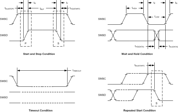 Figure 4. SMBus Timing Diagram
6.35 Typical Characteristics
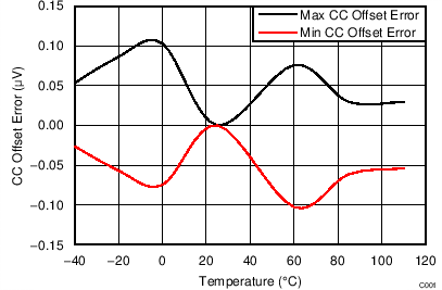
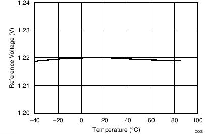
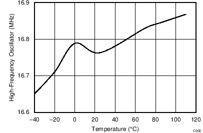
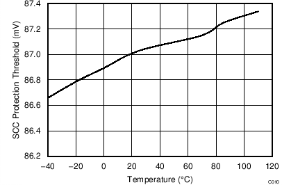
| Threshold setting is 88.85 mV. | ||
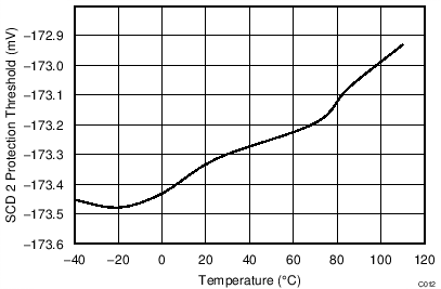
| Threshold setting is –177.7 mV. | ||
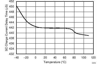
| Threshold setting is 465 µs. | ||
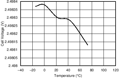
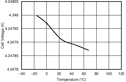
| This is the VCELL average for single cell. |
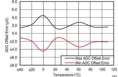
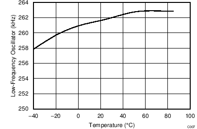
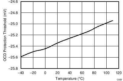
| Threshold setting is –25 mV. | ||
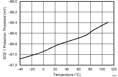
| Threshold setting is –88.85 mV. | ||
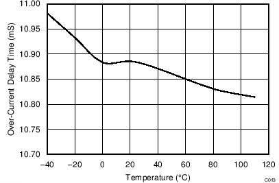
| Threshold setting is 11 ms. | ||
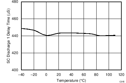
| Threshold setting is 465 µs (including internal delay). |
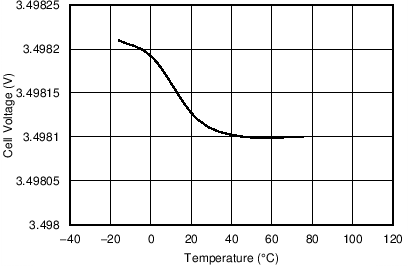
| This is the VCELL average for single cell. |
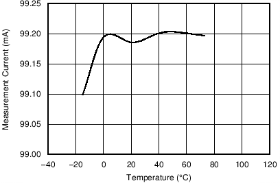
| ISET = 100 mA | ||