SWRS120E June 2011 – October 2014 CC1125
PRODUCTION DATA.
- 1Device Overview
- 2Revision History
- 3Terminal Configuration and Functions
-
4Specifications
- 4.1 Absolute Maximum Ratings
- 4.2 Handling Ratings
- 4.3 Recommended Operating Conditions (General Characteristics)
- 4.4 Thermal Resistance Characteristics for RHB Package
- 4.5 RF Characteristics
- 4.6 Regulatory Standards
- 4.7 Current Consumption, Static Modes
- 4.8 Current Consumption, Transmit Modes
- 4.9 Current Consumption, Receive Modes
- 4.10
Receive Parameters
- 4.10.1 General Receive Parameters (High-Performance Mode)
- 4.10.2 RX Performance in 950-MHz Band (High-Performance Mode)
- 4.10.3 RX Performance in 868-, 915-, and 920-MHz Bands (High-Performance Mode)
- 4.10.4 RX Performance in 434-MHz Band (High-Performance Mode)
- 4.10.5 RX Performance in 169-MHz Band (High-Performance Mode)
- 4.10.6 RX Performance in Low-Power Mode
- 4.11 Transmit Parameters
- 4.12 PLL Parameters
- 4.13 Wake-up and Timing
- 4.14 High-Speed Crystal Oscillator
- 4.15 High-Speed Clock Input (TCXO)data to TCXO table
- 4.16 32-kHz Clock Input
- 4.17 Low Speed RC Oscillator
- 4.18 I/O and Reset
- 4.19 Temperature Sensor
- 4.20 Typical Characteristics
- 5Detailed Description
- 6Typical Application Circuit
- 7Device and Documentation Support
- 8Mechanical Packaging and Orderable Information
パッケージ・オプション
メカニカル・データ(パッケージ|ピン)
- RHB|32
サーマルパッド・メカニカル・データ
- RHB|32
発注情報
1 Device Overview
1.1 Features
- High-Performance, Single-Chip Transceiver
- Adjacent Channel Selectivity: 67 dB at
6.25-kHz Offset - Blocking Performance: 104 dB at 10 MHz
- Excellent Receiver Sensitivity
- –129 dBm at 300 bps
- –123 dBm at 1.2 kbps
- –110 dBm at 50 kbps
- Very Low Phase Noise: –115 dBc/Hz at
10-kHz Offset
- Adjacent Channel Selectivity: 67 dB at
- Suitable for Systems Targeting ETSI
Category 1 - Separate 128-Byte RX and TX FIFOs
- Support for Seamless Integration With the CC1190 Device for Increased Range Giving up to 3-dB Improvement in Sensitivity and up to +27-dBm Output Power
- High Spectral Efficiency (9.6 kbps in 12.5-kHz Channel in Compliance With FCC Narrowbanding Mandate)
- Power Supply
- Wide Supply Voltage Range (2.0 V to 3.6 V)
- Low Current Consumption:
- RX: 2 mA in RX Sniff Mode
- RX: 17 mA Peak Current in Low-Power Mode
- RX: 26 mA Peak Current in High-Performance Mode
- TX: 47 mA at +14 dBm
- Power Down: 0.12 μA (0.5 μA With Enhanced Wake-On-Radio (eWOR) Timer Running)
- Programmable Output Power up to +16 dBm With 0.4-dB Step Size
- Automatic Output Power Ramping
- Configurable Data Rates: 0 to 200 kbps
- Supported Modulation Formats: 2-FSK,
2-GFSK, 4-FSK, 4-GFSK, MSK, OOK - WaveMatch: Advanced Digital Signal Processing for Improved Sync Detect Performance
- RoHS-Compliant 5-mm x 5-mm No-Lead QFN
32-Pin Package (RHB) - Regulations – Suitable for Systems Targeting Compliance With
- Europe: ETSI EN 300 220 Category 1, ETSI EN 54-25, ETSI EN 300 113, and EN 301 166
- US: FCC CFR47 Part 15, 24, 90, 101
- Japan: ARIB RCR STD-T30, T-67, T-108
- Peripherals and Support Functions
- eWOR Functionality for Automatic Low-Power Receive Polling
- Includes Functions for Antenna Diversity Support
- Support for Retransmissions
- Support for Auto-Acknowledge of Received Packets
- TCXO Support and Control, also in Power Modes
- Automatic Clear Channel Assessment (CCA) for Listen-Before-Talk (LBT) Systems
- Built-in Coding Gain Support for Increased Range and Robustness
- Digital RSSI Measurement
- Temperature Sensor
1.2 Applications
- Social Alarms
- Narrowband Ultra-Low-Power Wireless Systems With Channel Spacing Down to 4 kHz
- 169-, 315-, 433-, 868-, 915-, 920-, 950-MHz ISM/SRD Band Systems
- Wireless Metering and Wireless Smart Grid (AMR and AMI)
- IEEE 802.15.4g Systems
- Home and Building Automation
- Wireless Alarm and Security Systems
- Industrial Monitoring and Control
- Wireless Healthcare Applications
- Wireless Sensor Networks and Active RFID
- Private Mobile Radios
1.3 Description
The CC1125 device is a fully integrated single-chip radio transceiver designed for high performance at very low-power and low-voltage operation in cost-effective wireless systems. All filters are integrated, thus removing the need for costly external SAW and IF filters. The device is mainly intended for the ISM (Industrial, Scientific and Medical) and SRD (Short Range Device) frequency bands at 164–192 MHz, 274–320 MHz, 410–480 MHz, and 820–960 MHz.
The CC1125 device provides extensive hardware support for packet handling, data buffering, burst transmissions, clear channel assessment, link quality indication, and Wake-On-Radio. The main operating parameters of the CC1125 device can be controlled through an SPI interface. In a typical system, the CC1125 device will be used with a microcontroller and only a few external passive components.
1.4 Functional Block Diagram
Figure 1-1 shows the system block diagram of the CC1125 device.
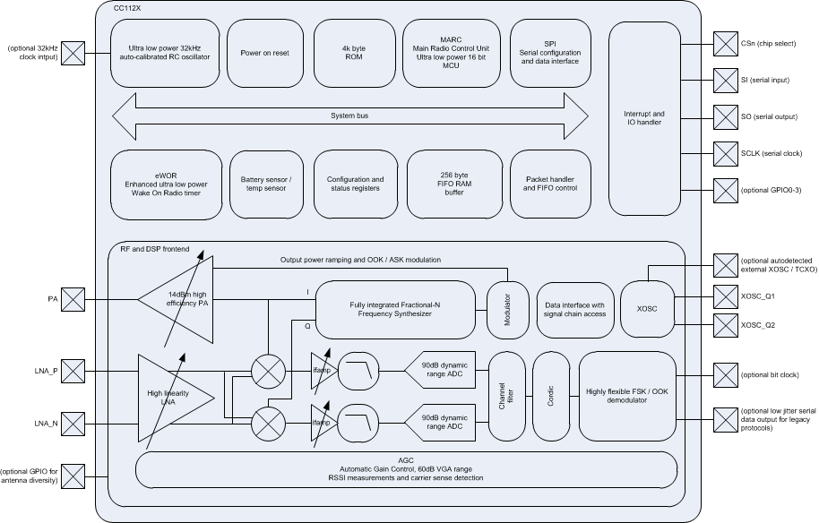 Figure 1-1 Functional Block Diagram