SWRS120E June 2011 – October 2014 CC1125
PRODUCTION DATA.
- 1Device Overview
- 2Revision History
- 3Terminal Configuration and Functions
-
4Specifications
- 4.1 Absolute Maximum Ratings
- 4.2 Handling Ratings
- 4.3 Recommended Operating Conditions (General Characteristics)
- 4.4 Thermal Resistance Characteristics for RHB Package
- 4.5 RF Characteristics
- 4.6 Regulatory Standards
- 4.7 Current Consumption, Static Modes
- 4.8 Current Consumption, Transmit Modes
- 4.9 Current Consumption, Receive Modes
- 4.10
Receive Parameters
- 4.10.1 General Receive Parameters (High-Performance Mode)
- 4.10.2 RX Performance in 950-MHz Band (High-Performance Mode)
- 4.10.3 RX Performance in 868-, 915-, and 920-MHz Bands (High-Performance Mode)
- 4.10.4 RX Performance in 434-MHz Band (High-Performance Mode)
- 4.10.5 RX Performance in 169-MHz Band (High-Performance Mode)
- 4.10.6 RX Performance in Low-Power Mode
- 4.11 Transmit Parameters
- 4.12 PLL Parameters
- 4.13 Wake-up and Timing
- 4.14 High-Speed Crystal Oscillator
- 4.15 High-Speed Clock Input (TCXO)data to TCXO table
- 4.16 32-kHz Clock Input
- 4.17 Low Speed RC Oscillator
- 4.18 I/O and Reset
- 4.19 Temperature Sensor
- 4.20 Typical Characteristics
- 5Detailed Description
- 6Typical Application Circuit
- 7Device and Documentation Support
- 8Mechanical Packaging and Orderable Information
パッケージ・オプション
メカニカル・データ(パッケージ|ピン)
- RHB|32
サーマルパッド・メカニカル・データ
- RHB|32
発注情報
4 Specifications
All measurements performed on CC1120EM_868_915 rev.1.0.1, CC1120EM_955 rev.1.2.1, CC1120EM_420_470 rev.1.0.1 or CC1120EM_169 rev.1.2 (fxosc = 32 MHz), and CC1125EM_868_915 rev.1.1.0, CC1125EM_420_470 rev.1.1.0, CC1125EM_169 rev.1.1.0, CC1125EM-Cat1-868 (fxosc = 40 MHz).
4.1 Absolute Maximum Ratings(1)(2)
| PARAMETER | MIN | MAX | UNIT | CONDITION | |
|---|---|---|---|---|---|
| Supply voltage (VDD, AVDD_x) | –0.3 | 3.9 | V | All supply pins must have the same voltage | |
| Solder reflow temperature | 260 | °C | According to IPC/JEDEC J-STD-020 | ||
| Input RF level | +10 | dBm | |||
| Voltage on any digital pin | –0.3 | VDD+0.3 | V | max 3.9 | |
| Voltage on analog pins (including DCPL pins) |
–0.3 | 2.0 | V | ||
4.2 Handling Ratings
| MIN | MAX | UNIT | ||||
|---|---|---|---|---|---|---|
| Tstg | Storage temperature range | –40 | 125 | °C | ||
| VESD | Electrostatic discharge (ESD) performance: | Human body model (HBM), per ANSI/ESDA/JEDEC JS001(1) | –2 | 2 | kV | |
| Charged device model (CDM), per JESD22-C101(2) | All pins | –500 | 500 | V | ||
4.3 Recommended Operating Conditions (General Characteristics)
| PARAMETER | MIN | TYP | MAX | UNIT | CONDITION | |
|---|---|---|---|---|---|---|
| Voltage supply range | 2.0 | 3.6 | V | All supply pins must have the same voltage | ||
| Voltage on digital inputs | 0 | VDD | V | |||
| Temperature range | –40 | 85 | °C | Ambient | ||
4.4 Thermal Resistance Characteristics for RHB Package
| °C/W(1) | AIR FLOW (m/s)(2) | ||
|---|---|---|---|
| RθJC | Junction-to-case (top) | 21.1 | 0.00 |
| RθJB | Junction-to-board | 5.3 | 0.00 |
| RθJA | Junction-to-free air | 31.3 | 0.00 |
| PsiJT | Junction-to-package top | 0.2 | 0.00 |
| PsiJB | Junction-to-board | 5.3 | 0.00 |
| RθJC | Junction-to-case (bottom) | 0.8 | 0.00 |
- JESD51-2, Integrated Circuits Thermal Test Method Environmental Conditions - Natural Convection (Still Air)
- JESD51-3, Low Effective Thermal Conductivity Test Board for Leaded Surface Mount Packages
- JESD51-7, High Effective Thermal Conductivity Test Board for Leaded Surface Mount Packages
- JESD51-9, Test Boards for Area Array Surface Mount Package Thermal Measurements
4.5 RF Characteristics
| PARAMETER | MIN | TYP | MAX | UNIT | CONDITION | |
|---|---|---|---|---|---|---|
| Frequency bands | 820 | 960 | MHz | |||
| 410 | 480 | MHz | ||||
| (273.3) | (320) | MHz | See SWRA398 for more information. | |||
| 164 | 192 | MHz | ||||
| (205) | (240) | MHz | Contact TI for more information about the use of these frequency bands. | |||
| (136.7) | (160) | MHz | ||||
| Frequency resolution | 30 | Hz | In 820–950 MHz band | |||
| 15 | Hz | In 410–480 MHz band | ||||
| 6 | Hz | In 164–192 MHz band | ||||
| Data rate | 0 | 200 | kbps | Packet mode | ||
| 0 | 100 | kbps | Transparent mode | |||
| Data rate step size | 1e-4 | bps | ||||
4.6 Regulatory Standards
| PERFORMANCE MODE | Frequency Band | Suitable for compliance with | Comments | |
|---|---|---|---|---|
| High-performance mode | 820–960 MHz | ARIB T-108 ARIB T-96 ETSI EN 300 220 category 1 ETSI EN 54-25 FCC PART 101 FCC PART 24 SUBMASK D FCC PART 15.247 FCC PART 15.249 FCC PART 90 MASK G FCC PART 90 MASK J |
Performance also suitable for systems targeting maximum allowed output power in the respective bands, using a range extender such as the CC1190 device | |
| 410–480 MHz | ARIB T-67 ARIB RCR STD-30 ETSI EN 301 166 ETSI EN 300 113 ETSI EN 300 220 category 1 FCC PART 90 MASK D FCC PART 90 MASK E FCC PART 90 MASK G |
Performance also suitable for systems targeting maximum allowed output power in the respective bands, using a range extender | ||
| 164–192 MHz | ETSI EN 300 220 category 1 ETSI EN 301 166 ETSI EN 300 113 FCC PART 90 MASK C FCC PART 90 MASK D FCC PART 90 MASK E |
Performance also suitable for systems targeting maximum allowed output power in the respective bands, using a range extender | ||
| Low-power mode | 820–960 MHz | ETSI EN 300 220 category 2 FCC PART 15.247 FCC PART 15.249 |
||
| 410–480 MHz | ETSI EN 300 220 category 2 | |||
| 164–192 MHz | ETSI EN 300 220 category 2 | |||
4.7 Current Consumption, Static Modes
TA = 25°C, VDD = 3.0 V, fxosc = 32 MHz if nothing else stated.| PARAMETER | MIN | TYP | MAX | UNIT | CONDITION | |
|---|---|---|---|---|---|---|
| Power down with retention | 0.12 | 1 | µA | |||
| 0.5 | µA | Low-power RC oscillator running | ||||
| XOFF mode | 170 | µA | Crystal oscillator / TCXO disabled | |||
| IDLE mode | 1.3 | mA | Clock running, system waiting with no radio activity | |||
4.8 Current Consumption, Transmit Modes
4.8.1 950-MHz Band (High-Performance Mode)
TA = 25°C, VDD = 3.0 V, fxosc = 32 MHz if nothing else stated
| PARAMETER | MIN | TYP | MAX | UNIT | CONDITION |
|---|---|---|---|---|---|
| TX current consumption +10 dBm | 37 | mA | |||
| TX current consumption 0 dBm | 26 | mA |
4.8.2 868-, 915-, and 920-MHz Bands (High-Performance Mode)
TA = 25°C, VDD = 3.0 V, fxosc = 40 MHz if nothing else stated
| PARAMETER | MIN | TYP | MAX | UNIT | CONDITION | |
|---|---|---|---|---|---|---|
| TX current consumption +14 dBm | 47 | mA | ||||
| TX current consumption +10 dBm | 38 | mA | ||||
4.8.3 434-MHz Band (High-Performance Mode)
TA = 25°C, VDD = 3.0 V, fxosc = 40 MHz if nothing else stated
| PARAMETER | MIN | TYP | MAX | UNIT | CONDITION | |
|---|---|---|---|---|---|---|
| TX current consumption +15 dBm | 51 | mA | ||||
| TX current consumption +14 dBm | 47 | mA | ||||
| TX current consumption +10 dBm | 36 | mA | ||||
4.8.4 169-MHz Band (High Performance Mode)
TA = 25°C, VDD = 3.0 V, fxosc = 40 MHz if nothing else stated
| PARAMETER | MIN | TYP | MAX | UNIT | CONDITION | |
|---|---|---|---|---|---|---|
| TX current consumption +15 dBm | 56 | mA | ||||
| TX current consumption +14 dBm | 52 | mA | ||||
| TX current consumption +10 dBm | 40 | mA | ||||
4.8.5 Low-Power Mode
TA = 25°C, VDD = 3.0 V, fc = 869.5 MHz, fxosc = 32 MHz if nothing else stated
| PARAMETER | MIN | TYP | MAX | UNIT | CONDITION | |
|---|---|---|---|---|---|---|
| TX current consumption +10 dBm | 32 | mA | ||||
4.9 Current Consumption, Receive Modes
4.9.1 High-Performance Mode
TA = 25°C, VDD = 3.0 V, fc = 869.5 MHz, fxosc = 32 MHz if nothing else stated
| PARAMETER | MIN | TYP | MAX | UNIT | CONDITION | |
|---|---|---|---|---|---|---|
| RX wait for sync | Using RX sniff mode, where the receiver wakes up at regular intervals to look for an incoming packet | |||||
| 1.2 kbps, 4-byte preamble | 2 | mA | ||||
| 38.4 kbps, 4-byte preamble | 13.4 | mA | ||||
| RX peak current, fxosc = 40 MHz | Peak current consumption during packet reception at the sensitivity threshold | |||||
| 433-, 868-, 915-, and 920-MHz bands | 26 | mA | ||||
| 169-MHz band | 27 | mA | ||||
| Average current consumption Check for data packet every 1 second using wake on radio |
15 | µA | 50 kbps, 5-byte preamble, 40-kHz RC oscillator used as sleep timer | |||
4.9.2 Low-Power Mode
TA = 25°C, VDD = 3.0 V, fc = 869.5 MHz, fxosc = 32 MHz if nothing else stated
| PARAMETER | MIN | TYP | MAX | UNIT | CONDITION | |
|---|---|---|---|---|---|---|
| RX peak current low-power RX mode 1.2 kbps |
17 | mA | Peak current consumption during packet reception at the sensitivity level | |||
4.10 Receive Parameters
All RX measurements made at the antenna connector, to a bit error rate (BER) limit of 1%.
4.10.1 General Receive Parameters (High-Performance Mode)
TA = 25°C, VDD = 3.0 V, fc = 869.5 MHz if nothing else stated
| PARAMETER | MIN | TYP | MAX | UNIT | CONDITION | |
|---|---|---|---|---|---|---|
| Saturation | +10 | dBm | ||||
| Digital channel filter programmable bandwidth | ||||||
| fxosc = 32 MHz | 2.8 | 200 | kHz | |||
| fxosc = 40 MHz | 3.5 | 250 | kHz | |||
| IIP3, normal mode | –14 | dBm | At maximum gain | |||
| IIP3, high linearity mode | –8 | dBm | Using 6-dB gain reduction in front end | |||
| Datarate offset tolerance | ±12 | % | With carrier sense detection enabled and assuming 4-byte preamble | |||
| ±0.2 | % | With carrier sense detection disabled | ||||
| Spurious emissions | Radiated emissions measured according to ETSI EN 300 220, fc = 869.5 MHz | |||||
| 1–13 GHz (VCO leakage at 3.5 GHz) | –56 | dBm | ||||
| 30 MHz to 1 GHz | < –57 | dBm | ||||
| Optimum source impedance | (Differential or single-ended RX configurations) | |||||
| 868-, 915-, and 920-MHz bands | 60 + j60 / 30 + j30 | Ω | ||||
| 433-MHz band | 100 + j60 / 50+ j30 | Ω | ||||
| 169-MHz band | 140 + j40 / 70 + j20 | Ω | ||||
4.10.2 RX Performance in 950-MHz Band (High-Performance Mode)
TA = 25°C, VDD = 3.0 V, fxosc = 32 MHz if nothing else stated
| PARAMETER | MIN | TYP | MAX | UNIT | CONDITION |
|---|---|---|---|---|---|
| Sensitivity Note: Sensitivity can be improved if the TX and RX matching networks are separated. |
–120 | dBm | 1.2 kbps, DEV=4 kHz CHF=10 kHz(1) | ||
| –107 | dBm | 50 kbps 2GFSK, DEV=25 kHz, CHF=100 kHz | |||
| –100 | dBm | 200 kbps, DEV=83 kHz (outer symbols), CHF=200 kHz, 4GFSK(2) | |||
| Blocking and Selectivity 1.2 kbps 2-FSK, 12.5-kHz channel separation, 4-kHz deviation, 10-kHz channel filter |
51 | dB | ± 12.5 kHz (adjacent channel) | ||
| 52 | dB | ± 25 kHz (alternate channel) | |||
| 73 | dB | ± 1 MHz | |||
| 76 | dB | ± 2 MHz | |||
| 81 | dB | ± 10 MHz | |||
| Blocking and Selectivity 50 kbps 2-GFSK, 200-kHz channel separation, 25-kHz deviation, 100-kHz channel filter (Same modulation format as 802.15.4g Mandatory Mode) |
43 | dB | ± 200 kHz (adjacent channel) | ||
| 51 | dB | ± 400 kHz (alternate channel) | |||
| 62 | dB | ± 1 MHz | |||
| 65 | dB | ± 2 MHz | |||
| 71 | dB | ± 10 MHz | |||
| Blocking and Selectivity 200 kbps 4-GFSK, 83-kHz deviation (outer symbols), 200-kHz channel filter, zero IF |
37 | dB | ± 200 kHz (adjacent channel) | ||
| 44 | dB | ± 400 kHz (alternate channel) | |||
| 55 | dB | ± 1 MHz | |||
| 58 | dB | ± 2 MHz | |||
| 64 | dB | ± 10 MHz |
4.10.3 RX Performance in 868-, 915-, and 920-MHz Bands (High-Performance Mode)
TA = 25°C, VDD = 3.0 V, fxosc = 32 MHz if nothing else stated if nothing else stated
| PARAMETER | MIN | TYP | MAX | UNIT | CONDITION |
|---|---|---|---|---|---|
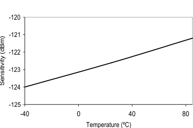
| Sensitivity | –129 | dBm | 300 bps, DEV=1 kHz CHF=3.8 kHz(1), fxosc = 40 MHz |
||
| –123 | dBm | 1.2 kbps, DEV=20 kHz CHF=50 kHz | |||
| –114 | dBm | 4.8 kbps OOK | |||
| –110 | dBm | 38.4 kbps, DEV=20 kHz CHF=100 kHz | |||
| –110 | dBm | 50 kbps 2GFSK, DEV=25 kHz, CHF=100 kHz | |||
| –103 | dBm | 200 kbps, DEV=83 kHz (outer symbols), CHF=200 kHz, 4GFSK | |||
| Blocking and Selectivity 0.3-kbps 2-FSK, 6.25-kHz channel separation, 1-kHz deviation, 3.8-kHz channel filter fxosc = 40 MHz using TCXO |
62 | dB | ± 6.25 kHz (adjacent channel) | ||
| 63 | dB | ± 12.5 kHz (alternate channel) | |||
| 83 | dB | ± 1 MHz | |||
| 87 | dB | ± 2 MHz | |||
| 91 | dB | ± 10 MHz | |||
| Blocking and Selectivity 1.2-kbps 2-FSK, 12.5-kHz channel separation, 4-kHz deviation, 10-kHz channel filter fxosc = 40 MHz using TCXO |
58 | dB | + 12.5 kHz (adjacent channel) | ||
| 58 | dB | ± 25 kHz (alternate channel) | |||
| 78 | dB | ± 1 MHz | |||
| 82 | dB | ± 2 MHz | |||
| 86 | dB | ± 10 MHz | |||
| Blocking and Selectivity 1.2-kbps 2-GFSK, 25-kHz channel separation, 4-kHz deviation, 16-kHz channel filter fxosc = 40 MHz using TCXO Using external SAW filter for compliance with ETSI category 1 |
58 | dB | ± 25 kHz (alternate channel) | ||
| 77 | dB | ± 1 MHz | |||
| 106 | dB | ± 2 MHz | |||
| 101 | dB | ± 10 MHz | |||
| Blocking and Selectivity 38.4-kbps 2-GFSK, 100-kHz channel separation, 20-kHz deviation, 100-kHz channel filter |
42 | dB | ± 100 kHz (adjacent channel) | ||
| 43 | dB | ± 200 kHz (alternate channel) | |||
| 62 | dB | ± 1 MHz | |||
| 66 | dB | ± 2 MHz | |||
| 74 | dB | ± 10 MHz | |||
| Blocking and Selectivity 50-kbps 2-GFSK, 200-kHz channel separation, 25-kHz deviation, 100-kHz channel filter (Same modulation format as 802.15.4g Mandatory Mode) |
43 | dB | ± 200 kHz (adjacent channel) | ||
| 50 | dB | ± 400 kHz (alternate channel) | |||
| 61 | dB | ± 1 MHz | |||
| 65 | dB | ± 2 MHz | |||
| 74 | dB | ± 10 MHz | |||
| Blocking and Selectivity 200-kbps 4-GFSK, 83-kHz deviation (outer symbols), 200-kHz channel filter, zero IF |
36 | dB | ± 200 kHz (adjacent channel) | ||
| 44 | dB | ± 400 kHz (alternate channel) | |||
| 55 | dB | ± 1 MHz | |||
| 59 | dB | ± 2 MHz | |||
| 67 | dB | ± 10 MHz | |||
| Image rejection (Image compensation enabled) fxosc = 40 MHz using TCXO |
58 | dB | 1.2 kbps, DEV=4 kHz CHF=10 kHz(1), image at -125 kHz |
4.10.4 RX Performance in 434-MHz Band (High-Performance Mode)
TA = 25°C, VDD = 3.0 V, fxosc = 32 MHz if nothing else stated if nothing else stated
| PARAMETER | MIN | TYP | MAX | UNIT | CONDITION |
|---|---|---|---|---|---|
| Sensitivity | –129 | dBm | 300 bps, DEV=1 kHz, CHF=3.8 kHz(1)
fxosc = 40 MHz |
||
| –123 | dBm | 1.2 kbps, DEV=4 kHz CHF=10 kHz(1) | |||
| –109 | dBm | 50-kbps 2-GFSK, DEV=25 kHz, CHF=100 kHz(1) | |||
| –116 | dBm | 1.2 kbps, DEV=20 kHz CHF=50 kHz(1) | |||
| Blocking and Selectivity 0.3-kbps 2-FSK, 6.25-kHz channel separation, 1-kHz deviation, 3.8-kHz channel filter fxosc = 40 MHz using TCXO |
65 | dB | + 6.25 kHz (adjacent channel) | ||
| 66 | dB | + 12.5 kHz (alternate channel) | |||
| 86 | dB | ± 1 MHz | |||
| 90 | dB | ± 2 MHz | |||
| 95 | dB | ± 10 MHz | |||
| Blocking and Selectivity 1.2-kbps 2-FSK, 12.5-kHz channel separation, 4-kHz deviation, 10-kHz channel filter fxosc = 40 MHz using TCXO |
60 | dB | + 12.5 kHz (adjacent channel) | ||
| 61 | dB | ± 25 kHz (alternate channel) | |||
| 80 | dB | ± 1 MHz | |||
| 85 | dB | ± 2 MHz | |||
| 91 | dB | ± 10 MHz | |||
| Blocking and Selectivity 38.4-kbps 2-GFSK, 100-kHz channel separation, 20-kHz deviation, 100-kHz channel filter |
47 | dB | + 100 kHz (adjacent channel) | ||
| 50 | dB | ± 200 kHz (alternate channel) | |||
| 67 | dB | ± 1 MHz | |||
| 71 | dB | ± 2 MHz | |||
| 78 | dB | ± 10 MHz |
4.10.5 RX Performance in 169-MHz Band (High-Performance Mode)
TA = 25°C, VDD = 3.0 V, fxosc = 32 MHz if nothing else stated
| PARAMETER | MIN | TYP | MAX | UNIT | CONDITION |
|---|---|---|---|---|---|
| Sensitivity | –129 | dBm | 300 bps, DEV=1 kHz, CHF=3.8 kHz(1)
fxosc = 40 MHz |
||
| –123 | dBm | 1.2 kbps, DEV=4 kHz CHF=10 kHz(1) | |||
| Blocking and Selectivity 0.3-kbps 2-FSK, 6.25-kHz channel separation, 1-kHz deviation, 3.8-kHz channel filter fxosc = 40 MHz using TCXO |
67 | dB | ± 6.25 kHz (adjacent channel) | ||
| 67 | dB | + 12.5 kHz (alternate channel) | |||
| 88 | dB | ± 1 MHz | |||
| 101 | dB | –2 MHz | |||
| 104 | dB | ± 10 MHz | |||
| Blocking and Selectivity 1.2-kbps 2-FSK, 12.5-kHz channel separation, 4-kHz deviation, 10-kHz channel filter fxosc = 40 MHz using TCXO |
63 | dB | ± 12.5 kHz (adjacent channel) | ||
| 65 | dB | ± 25 kHz (alternate channel) | |||
| 82 | dB | ± 1 MHz | |||
| 86 | dB | ± 2 MHz | |||
| 93 | dB | –10 MHz | |||
| Spurious Response Rejection 1.2-kbps 2-FSK, 12.5-kHz channel separation, 4-kHz deviation, 10-kHz channel filter |
70 | dB | |||
| Image Rejection (Image compensation enabled) |
66 | dB | 1.2 kbps, DEV=4 kHz CHF=10 kHz(1), image at –125 kHz |
4.10.6 RX Performance in Low-Power Mode
TA = 25°C, VDD = 3.0 V, fc = 869.5 MHz, fxosc = 32 MHz if nothing else stated
| PARAMETER | MIN | TYP | MAX | UNIT | CONDITION |
|---|---|---|---|---|---|
| Sensitivity | –111 | dBm | 1.2 kbps, DEV=4 kHz CHF=10 kHz(1) | ||
| –99 | dBm | 38.4 kbps, DEV=50 kHz CHF=100 kHz(1) | |||
| –99 | dBm | 50-kbps 2-GFSK, DEV=25 kHz, CHF=100 kHz(1) | |||
| Blocking and Selectivity 1.2-kbps 2-FSK, 12.5-kHz channel separation, 4-kHz deviation, 10-kHz channel filter |
46 | dB | ± 12.5 kHz (adjacent channel) | ||
| 46 | dB | ± 25 kHz (alternate channel) | |||
| 73 | dB | ± 1 MHz | |||
| 78 | dB | ± 2 MHz | |||
| 79 | dB | ± 10 MHz | |||
| Blocking and Selectivity 1.2-kbps 2-FSK, 50-kHz channel separation, 20-kHz deviation, 50-kHz channel filter |
43 | dB | ± 50 kHz (adjacent channel) | ||
| 45 | dB | + 100 kHz (alternate channel) | |||
| 71 | dB | ± 1 MHz | |||
| 74 | dB | ± 2 MHz | |||
| 75 | dB | ± 10 MHz | |||
| Blocking and Selectivity 38.4-kbps 2-GFSK, 100-kHz channel separation, 20-kHz deviation, 100-kHz channel filter |
37 | dB | + 100 kHz (adjacent channel) | ||
| 43 | dB | + 200 kHz (alternate channel) | |||
| 58 | dB | ± 1 MHz | |||
| 62 | dB | ± 2 MHz | |||
| 64 | dB | + 10 MHz | |||
| Blocking and Selectivity 50-kbps 2-GFSK, 200-kHz channel separation, 25-kHz deviation, 100-kHz channel filter (Same modulation format as 802.15.4g Mandatory Mode) |
43 | dB | + 200 kHz (adjacent channel) | ||
| 52 | dB | + 400 kHz (alternate channel) | |||
| 60 | dB | ± 1 MHz | |||
| 64 | dB | ± 2 MHz | |||
| 65 | dB | ± 10 MHz | |||
| Saturation | +10 | dBm |
4.11 Transmit Parameters
TA = 25°C, VDD = 3.0 V, fc = 869.5 MHz, fxosc = 32 MHz if nothing else stated
| PARAMETER | MIN | TYP | MAX | UNIT | CONDITION |
|---|---|---|---|---|---|
| Max output power | +12 | dBm | At 950 MHz | ||
| +14 | dBm | At 915- and 920-MHz | |||
| +15 | dBm | At 915- and 920-MHz with VDD = 3.6 V | |||
| +15 | dBm | At 868 MHz | |||
| +16 | dBm | At 868 MHz with VDD = 3.6 V | |||
| +15 | dBm | At 433 MHz | |||
| +16 | dBm | At 433 MHz with VDD = 3.6 V | |||
| +15 | dBm | At 169 MHz | |||
| +16 | dBm | At 169 MHz with VDD = 3.6 V | |||
| Min output power | –11 | dBm | Within fine step size range | ||
| –40 | dBm | Within coarse step size range | |||
| Output power step size | 0.4 | dB | Within fine step size range | ||
| Adjacent channel power | –75 | dBc | 4-GFSK 9.6 kbps in 12.5-kHz channel, measured in 100-Hz bandwidth at 434 MHz (FCC Part 90 Mask D compliant) | ||
| –58 | dBc | 4-GFSK 9.6 kbps in 12.5-kHz channel, measured in 8.75-kHz bandwidth (ETSI 300 220 compliant) | |||
| –61 | dBc | 2-GFSK 2.4 kbps in 12.5-kHz channel, 1.2-kHz deviation | |||
| Spurious emissions (not including harmonics) |
<–60 | dBm | |||
| Harmonics | Transmission at +14 dBm (or maximum allowed in applicable band where this is less than +14 dBm) using TI reference design. Emissions measured according to ARIB T-96 in 950-MHz band, ETSI EN 300-220 in 169-, 433-, and 868-MHz bands and FCC part 15.247 in 450- and 915-MHz band. Fourth harmonic in 915-MHz band will require extra filtering to meet FCC requirements if transmitting for long intervals (>50-ms periods). |
||||
| Second Harm, 169 MHz | –39 | dBm | |||
| Third Harm, 169 MHz | –58 | dBm | |||
| Second Harm, 433 MHz | –56 | dBm | |||
| Third Harm, 433 MHz | –51 | dBm | |||
| Second Harm, 450 MHz | –60 | dBm | |||
| Third Harm, 450 MHz | –45 | dBm | |||
| Second Harm, 868 MHz | –40 | dBm | |||
| Third Harm, 868 MHz | –42 | dBm | |||
| Second Harm, 915 MHz | 56 | dBuV/m | |||
| Third Harm, 915 MHz | 52 | dBuV/m | |||
| Fourth Harm, 915 MHz | 60 | dBuV/m | |||
| Second Harm, 950 MHz | –58 | dBm | |||
| Third Harm, 950 MHz | –42 | dBm | |||
| Optimum load | |||||
| Impedance 868-, 915-, and 920-MHz bands | 35 + j35 | Ω | |||
| 433-MHz band | 55 + j25 | Ω | |||
| 169-MHz band | 80 + j0 | Ω | |||
4.12 PLL Parameters
4.12.1 High-Performance Mode
TA = 25°C, VDD = 3.0 V, fc = 869.5 MHz, fxosc = 40 MHz using TCXO if nothing else stated
| PARAMETER | MIN | TYP | MAX | UNIT | CONDITION |
|---|---|---|---|---|---|
| Phase noise in 950-MHz band fxosc = 32 MHz |
–100 | dBc/Hz | ± 10 kHz offset | ||
| –103 | dBc/Hz | ± 100 kHz offset | |||
| –123 | dBc/Hz | ± 1 MHz offset | |||
| Phase noise in 868-, 915-, 920-MHz bands | –101 | dBc/Hz | ± 10 kHz offset | ||
| –102 | dBc/Hz | ± 100 kHz offset | |||
| –124 | dBc/Hz | ± 1 MHz offset | |||
| Phase noise in 433-MHz band | –107 | dBc/Hz | ± 10 kHz offset | ||
| –110 | dBc/Hz | ± 100 kHz offset | |||
| –130 | dBc/Hz | ± 1 MHz offset | |||
| Phase noise in 169-MHz band | –115 | dBc/Hz | ± 10 kHz offset | ||
| –115 | dBc/Hz | ± 100 kHz offset | |||
| –135 | dBc/Hz | ± 1 MHz offset |
4.12.2 Low-Power Mode
TA = 25°C, VDD = 3.0 V, fc = 869.5 MHz, fxosc = 32 MHz if nothing else stated
| PARAMETER | MIN | TYP | MAX | UNIT | CONDITION |
|---|---|---|---|---|---|
| Phase noise in 950-MHz band | –90 | dBc/Hz | ± 10 kHz offset | ||
| –92 | dBc/Hz | ± 100 kHz offset | |||
| –124 | dBc/Hz | ± 1 MHz offset | |||
| Phase noise in 868-, 915- , and 920-MHz bands | –95 | dBc/Hz | ± 10 kHz offset | ||
| –95 | dBc/Hz | ± 100 kHz offset | |||
| –124 | dBc/Hz | ± 1 MHz offset | |||
| Phase noise in 433-MHz band | –98 | dBc/Hz | ± 10 kHz offset | ||
| –102 | dBc/Hz | ± 100 kHz offset | |||
| –129 | dBc/Hz | ± 1 MHz offset | |||
| Phase noise in 169-MHz band | –106 | dBc/Hz | ± 10 kHz offset | ||
| –110 | dBc/Hz | ± 100 kHz offset | |||
| –136 | dBc/Hz | ± 1 MHz offset |
4.13 Wake-up and Timing
TA = 25°C, VDD = 3.0 V, fc = 869.5 MHz, fxosc = 32 MHz if nothing else stated
| PARAMETER | MIN | TYP | MAX | UNIT | CONDITION |
|---|---|---|---|---|---|
| Powerdown to IDLE | 0.4 | ms | Depends on crystal | ||
| IDLE to RX/TX | 166 | µs | Calibration disabled | ||
| 461 | µs | Calibration enabled | |||
| RX/TX turnaround | 50 | µs | |||
| RX/TX to IDLE time | 296 | µs | Calibrate when leaving RX/TX enabled | ||
| 0 | µs | Calibrate when leaving RX/TX disabled | |||
| Frequency synthesizer calibration | 391 | µs | When using SCAL strobe | ||
| Minimum required number of preamble bytes | 0.5 | bytes | Required for RF front-end gain settling only. Digital demodulation does not require preamble for settling. | ||
| Time from start RX until valid RSSI, including gain settling (function of channel bandwidth. Programmable for trade-off between speed and accuracy) |
4.6 | ms | 12.5-kHz channels | ||
| 0.3 | ms | 200-kHz channels |
4.14 High-Speed Crystal Oscillator
TA = 25°C, VDD = 3.0 V if nothing else stated
| PARAMETER | MIN | TYP | MAX | UNIT | CONDITION |
|---|---|---|---|---|---|
| Crystal frequency | 32 | 44 | MHz | It is expected that there will be degraded sensitivity at multiples of XOSC/2 in RX, and an increase in spurious emissions when the RF channel is close to multiples of XOSC in TX. We recommend that the RF channel is kept RX_BW/2 away from XOSC/2 in RX, and that the level of spurious emissions be evaluated if the RF channel is closer than 1 MHz to multiples of XOSC in TX. | |
| Load capacitance (CL) | 10 | pF | |||
| ESR | <50 | Ω | |||
| Start-up time | 0.4 | ms | Depends on crystal |
4.15 High-Speed Clock Input (TCXO)
TA = 25°C, VDD = 3.0 V if nothing else stated
| PARAMETER | MIN | TYP | MAX | UNIT | CONDITION |
|---|---|---|---|---|---|
| Clock frequency | 32 | 44 | MHz | ||
| TCXO with CMOS output | TCXO with CMOS output directly coupled to pin EXT_OSC | ||||
| High input voltage | 1.4 | VDD | V | ||
| Low input voltage | 0 | 0.6 | V | ||
| Rise / Fall time | 2 | ns | |||
| Clipped sine output | TCXO clipped sine output connected to pin EXT_OSC through series capacitor | ||||
| Clock input amplitude (peak-to-peak) | 0.8 | 1.5 | V |
4.16 32-kHz Clock Input
TA = 25°C, VDD = 3.0 V if nothing else stated
| PARAMETER | MIN | TYP | MAX | UNIT | CONDITION |
|---|---|---|---|---|---|
| Clock frequency | 32 | kHz | |||
| 32-kHz clock input pin input high voltage | 0.8×VDD | V | |||
| 32-kHz clock input pin input low voltage | 0.2×VDD | V |
4.17 Low Speed RC Oscillator
TA = 25°C, VDD = 3.0 V if nothing else stated
| PARAMETER | MIN | TYP | MAX | UNIT | CONDITION |
|---|---|---|---|---|---|
| Frequency | 32/40 | kHz | After calibration (calibrated against the high-speed XOSC) | ||
| Frequency accuracy after calibration | ±0.1 | % | Relative to frequency reference (for example, 32-MHz crystal or TCXO) | ||
| Initial calibration time | 1.6 | ms |
4.18 I/O and Reset
TA = 25°C, VDD = 3.0 V if nothing else stated
| PARAMETER | MIN | TYP | MAX | UNIT | CONDITION |
|---|---|---|---|---|---|
| Logic input high voltage | 0.8×VDD | V | |||
| Logic input low voltage | 0.2×VDD | V | |||
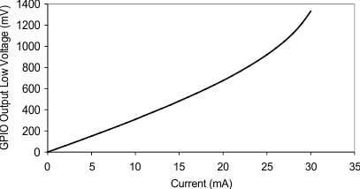
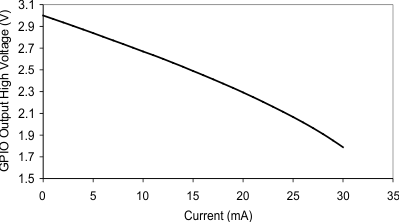
| Logic output high voltage | 0.8×VDD | V | At 4-mA output load or less | ||
| Logic output low voltage | 0.2×VDD | V | |||
| Power-on reset threshold | 1.3 | V | Voltage on DVDD pin |
4.19 Temperature Sensor
TA = 25°C, VDD = 3.0 V if nothing else stated
| PARAMETER | MIN | TYP | MAX | UNIT | CONDITION |
|---|---|---|---|---|---|
| Temperature sensor range | –40 | 85 | °C | ||
| Temperature coefficient | 2.66 | mV / °C | Change in sensor output voltage versus change in temperature | ||
| Typical output voltage | 794 | mV | Typical sensor output voltage at TA = 25°C, VDD = 3.0 V | ||
| VDD coefficient | 1.17 | mV / V | Change in sensor output voltage versus change in VDD |
The CC1125 device can be configured to provide a voltage proportional to temperature on GPIO1. The temperature can be estimated by measuring this voltage (see Section 4.19, Temperature Sensor). For more information, see the temperature sensor design note (SWRA415).
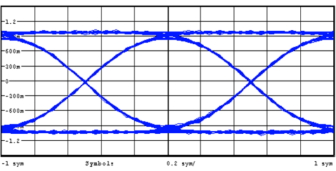
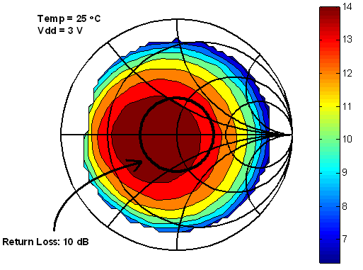
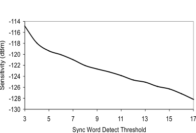
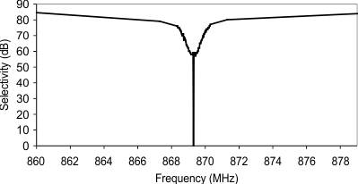
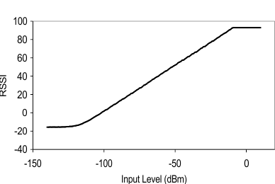
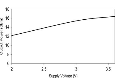
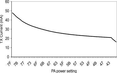
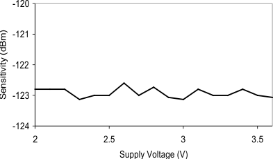
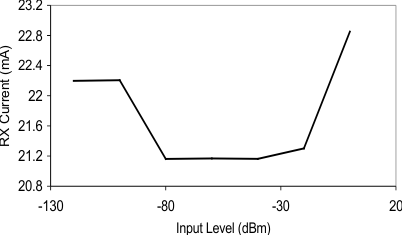
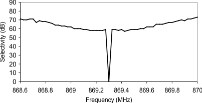
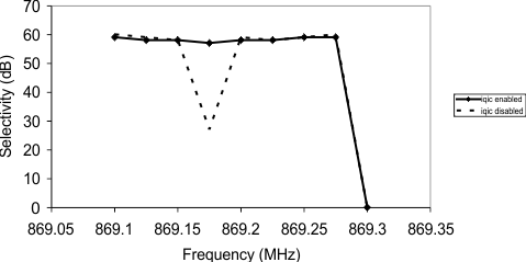
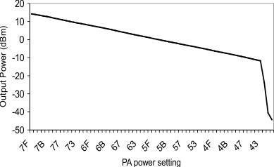
4.20 Typical Characteristics
TA = 25°C, VDD = 3.0 V, fc = 869.5 MHz if nothing else stated.
All measurements performed on CC1120EM_868_915 rev.1.0.1, CC1120EM_955 rev.1.2.1, CC1120EM_420_470 rev.1.0.1 or CC1120EM_169 rev.1.2 (fxosc = 32 MHz), and CC1125EM_868_915 rev.1.1.0, CC1125EM_420_470 rev.1.1.0, CC1125EM_169 rev.1.1.0, CC1125EM-Cat1-868 (fxosc = 40 MHz).
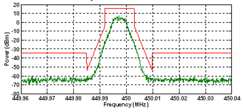
Figure 4-16 was measured at the 50-Ω antenna connector.
Max Setting, 170 MHz
vs PA Power Setting
vs PA Power Setting
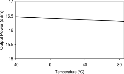
Max Setting, 170 MHz, 3.6 V