SCAS895B May 2010 – February 2017 CDCLVC1102 , CDCLVC1103 , CDCLVC1104 , CDCLVC1106 , CDCLVC1108 , CDCLVC1110 , CDCLVC1112
PRODUCTION DATA.
- 1 Features
- 2 Applications
- 3 Description
- 4 Revision History
- 5 Pin Configuration and Functions
- 6 Specifications
- 7 Parameter Measurement Information
- 8 Detailed Description
- 9 Application and Implementation
- 10Power Supply Recommendations
- 11Layout
- 12Device and Documentation Support
- 13Mechanical, Packaging, and Orderable Information
パッケージ・オプション
メカニカル・データ(パッケージ|ピン)
- PW|20
サーマルパッド・メカニカル・データ
- PW|20
発注情報
8 Detailed Description
8.1 Overview
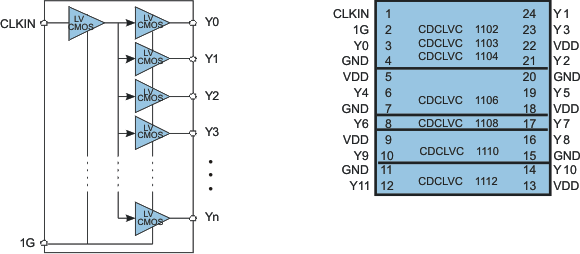
The CDCLVC11xx family of devices is a low-jitter and low-skew LVCMOS fan-out buffer solution. For best signal integrity, it is important to match the characteristic impedance of the CDCLVC11xx's output driver with that of the transmission line. Figure 5 and Figure 6 show the proper configuration per configuration for both VDD = 3.3 V and VDD = 2.5 V. TI recommends placing the series resistor close to the driver to minimize signal reflection.
8.2 Functional Block Diagram

Table 1. Output Logic Table
| INPUTS | OUTPUTS | |
|---|---|---|
| CLKIN | 1G | Yn |
| X | L | L |
| L | H | L |
| H | H | H |
8.3 Feature Description
The outputs of the CDCLVC11xx can be disabled by driving the asynchronous output enable pin (1G) low. Unused output can be left floating to reduce overall system component cost. All supply and ground pins must be connected to VDD and GND, respectively.
8.4 Device Functional Modes
The CDCLVC11xx operates from supplies between 2.5 V and 3.3 V.