JAJSD34C April 2017 – April 2018 CSD88599Q5DC
PRODUCTION DATA.
- 1特長
- 2アプリケーション
- 3概要
- 4改訂履歴
- 5Specifications
-
6Application and Implementation
- 6.1 Application Information
- 6.2 Brushless DC Motor With Trapezoidal Control
- 6.3 Power Loss Curves
- 6.4 Safe Operating Area (SOA) Curve
- 6.5 Normalized Power Loss Curves
- 6.6 Design Example – Regulate Current to Maintain Safe Operation
- 6.7 Design Example – Regulate Board and Case Temperature to Maintain Safe Operation
- 7Layout
- 8デバイスおよびドキュメントのサポート
- 9メカニカル、パッケージ、および注文情報
パッケージ・オプション
デバイスごとのパッケージ図は、PDF版データシートをご参照ください。
メカニカル・データ(パッケージ|ピン)
- DMM|22
サーマルパッド・メカニカル・データ
発注情報
5.6 Typical Power Block Device Characteristics
The typical power block system characteristic curves (Figure 1 through Figure 6) are based on measurements made on a PCB design with dimensions of 4 in (W) × 3.5 in (L) × 0.062 in (H) and 6 copper layers of 2-oz copper thickness. See Application and Implementation section for detailed explanation. TJ = 125°C, unless stated otherwise.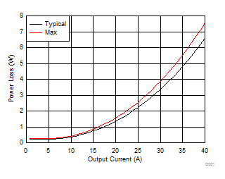
| VIN = 36 V | VDD = 10 V | D.C. = 50% | ||
| ƒSW = 20 kHz | L = 480 µH |
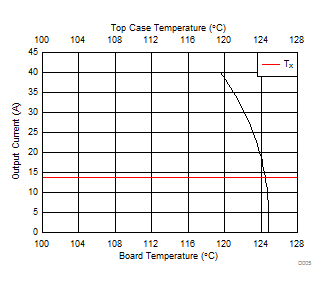
| VIN = 36 V | VDD = 10 V | D.C. = 50% | ||
| ƒSW = 20 kHz | L = 480 µH |
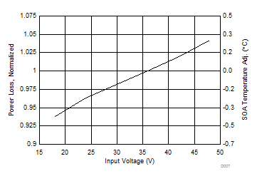
| D.C. = 50% | VDD = 10 V | IOUT = 40 A | ||
| ƒSW = 20 kHz | L = 480 µH |
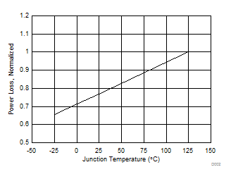
| VIN = 36 V | VDD = 10 V | D.C. = 50% | ||
| ƒSW = 20 kHz | L = 480 µH | IOUT = 40 A |
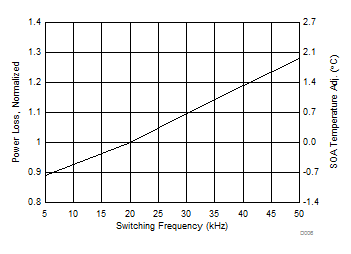
| VIN = 36 V | VDD = 10 V | IOUT = 40 A | ||
| L = 480 µH | D.C. = 50% |
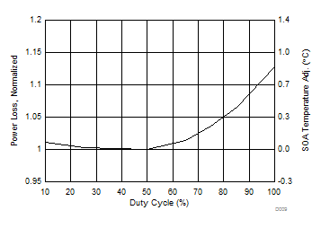
| VIN = 36 V | VDD = 10 V | |||
| ƒSW = 20 kHz | L = 480 µH |