JAJSHR1A July   2019  – December 2019 DAC43401 , DAC53401

PRODUCTION DATA.  

  1. 特長
  2. アプリケーション
  3. 概要
    1.     Device Images
      1.      機能ブロック図
      2.      DACx3401 による電源制御
  4. 改訂履歴
  5. Device Comparison Table
  6. Pin Configuration and Functions
    1.     Pin Functions
  7. Specifications
    1. 7.1  Absolute Maximum Ratings
    2. 7.2  ESD Ratings
    3. 7.3  Recommended Operating Conditions
    4. 7.4  Thermal Information
    5. 7.5  Electrical Characteristics
    6. 7.6  Timing Requirements: I2CTM Standard mode
    7. 7.7  Timing Requirements: I2CTM Fast mode
    8. 7.8  Timing Requirements: I2CTM Fast+ mode
    9. 7.9  Typical Characteristics: VDD = 1.8 V (Reference = VDD) or VDD = 2 V (Internal Reference)
    10. 7.10 Typical Characteristics: VDD = 5.5 V (Reference = VDD) or VDD = 5 V (Internal Reference)
    11. 7.11 Typical Characteristics
  8. Detailed Description
    1. 8.1 Overview
    2. 8.2 Functional Block Diagram
    3. 8.3 Feature Description
      1. 8.3.1 Digital-to-Analog Converter (DAC) Architecture
        1. 8.3.1.1 Reference Selection and DAC Transfer Function
          1. 8.3.1.1.1 Power Supply as Reference
          2. 8.3.1.1.2 Internal Reference
      2. 8.3.2 DAC Update
        1. 8.3.2.1 DAC Update Busy
      3. 8.3.3 Nonvolatile Memory (EEPROM or NVM)
        1. 8.3.3.1 NVM Cyclic Redundancy Check
        2. 8.3.3.2 NVM_CRC_ALARM_USER Bit
        3. 8.3.3.3 NVM_CRC_ALARM_INTERNAL Bit
      4. 8.3.4 Programmable Slew Rate
      5. 8.3.5 Power-on-Reset (POR)
      6. 8.3.6 Software Reset
      7. 8.3.7 Device Lock Feature
      8. 8.3.8 PMBus Compatibility
    4. 8.4 Device Functional Modes
      1. 8.4.1 Power Down Mode
      2. 8.4.2 Continuous Waveform Generation (CWG) Mode
      3. 8.4.3 PMBus Compatibility Mode
      4. 8.4.4 Medical Alarm Generation Mode
        1. 8.4.4.1 Low-Priority Alarm
        2. 8.4.4.2 Medium-Priority Alarm
        3. 8.4.4.3 High-Priority Alarm
        4. 8.4.4.4 Interburst Time
        5. 8.4.4.5 Pulse Off Time
        6. 8.4.4.6 Pulse On Time
    5. 8.5 Programming
      1. 8.5.1 F/S Mode Protocol
      2. 8.5.2 DACx3401 I2C Update Sequence
      3. 8.5.3 Address Byte
      4. 8.5.4 Command Byte
      5. 8.5.5 I2C Read Sequence
    6. 8.6 Register Map
      1. 8.6.1  STATUS Register (address = D0h) (reset = 000Ch or 0014h)
        1. Table 18. STATUS Register Field Descriptions
      2. 8.6.2  GENERAL_CONFIG Register (address = D1h) (reset = 01F0h)
        1. Table 19. GENERAL_CONFIG Register Field Descriptions
      3. 8.6.3  MED_ALARM_CONFIG Register (address = D2h) (reset = 0000h)
        1. Table 20. MED_ALARM_CONFIG Register Field Descriptions
      4. 8.6.4  TRIGGER Register (address = D3h) (reset = 0008h)
        1. Table 21. TRIGGER Register Field Descriptions
      5. 8.6.5  DAC_DATA Register (address = 21h) (reset = 0000h)
        1. Table 22. DAC_DATA Register Field Descriptions
      6. 8.6.6  DAC_MARGIN_HIGH Register (address = 25h) (reset = 0000h)
        1. Table 23. DAC_MARGIN_HIGH Register Field Descriptions
      7. 8.6.7  DAC_MARGIN_LOW Register (address = 26h) (reset = 0000h)
        1. Table 24. DAC_MARGIN_LOW Register Field Descriptions
      8. 8.6.8  PMBUS_OPERATION Register (address = 01h) (reset = 0000h)
        1. Table 25. PMBUS_OPERATION Register Field Descriptions
      9. 8.6.9  PMBUS_STATUS_BYTE Register (address = 78h) (reset = 0000h)
        1. Table 26. PMBUS_STATUS_BYTE Register Field Descriptions
      10. 8.6.10 PMBUS_VERSION Register (address = 98h) (reset = 2200h)
        1. Table 27. PMBUS_VERSION Register Field Descriptions
  9. Application and Implementation
    1. 9.1 Application Information
    2. 9.2 Typical Applications
      1. 9.2.1 Programmable LED Biasing
        1. 9.2.1.1 Design Requirements
        2. 9.2.1.2 Detailed Design Procedure
        3. 9.2.1.3 Application Curves
      2. 9.2.2 Power-Supply Margining
        1. 9.2.2.1 Design Requirements
        2. 9.2.2.2 Detailed Design Procedure
        3. 9.2.2.3 Application Curves
      3. 9.2.3 Medical Alarm Generation
        1. 9.2.3.1 Design Requirements
        2. 9.2.3.2 Detailed Design Procedure
        3. 9.2.3.3 Application Curves
  10. 10Power Supply Recommendations
  11. 11Layout
    1. 11.1 Layout Guidelines
    2. 11.2 Layout Example
  12. 12デバイスおよびドキュメントのサポート
    1. 12.1 ドキュメントのサポート
      1. 12.1.1 関連資料
    2. 12.2 関連リンク
    3. 12.3 ドキュメントの更新通知を受け取る方法
    4. 12.4 サポート・リソース
    5. 12.5 商標
    6. 12.6 静電気放電に関する注意事項
    7. 12.7 Glossary
  13. 13メカニカル、パッケージ、および注文情報

パッケージ・オプション

メカニカル・データ(パッケージ|ピン)
サーマルパッド・メカニカル・データ
発注情報

Typical Characteristics

at TA = 25°C, 10-bit DAC, and DAC outputs unloaded (unless otherwise noted)
DAC53401 DAC43401 SLASES7-Plot-021.gif
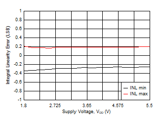
Reference = VDD
Figure 22. Integral Linearity Error vs Supply Voltage
DAC53401 DAC43401 SLASES7-Plot-023.gif
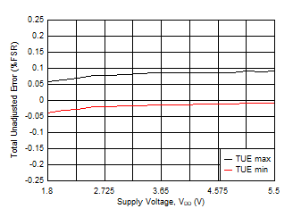
Reference = VDD
Figure 24. Total Unadjusted Error vs Supply Voltage
DAC53401 DAC43401 SLASES7-Plot-025.gif
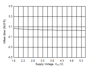
Reference = VDD
Figure 26. Offset Error vs Supply Voltage
DAC53401 DAC43401 SLASES7-Plot-027.gif
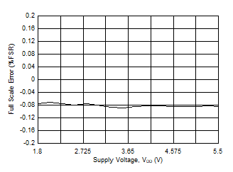
Reference = VDD
Figure 28. Full-Scale Error vs Supply Voltage
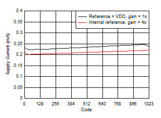
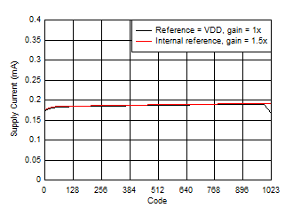
DAC53401 DAC43401 SLASES7-Plot-036.gif
VDD = 5.5 V
Figure 30. Supply Current vs Digital Input Code
DAC53401 DAC43401 SLASES7-Plot-038.gif
Internal reference (gain = 4x), DAC at midscale
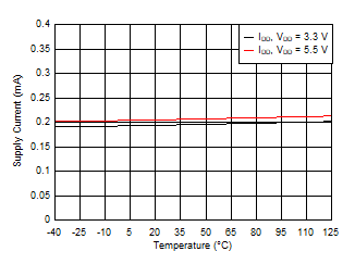
Figure 32. Supply Current vs Temperature
DAC53401 DAC43401 SLASES7-Plot-040.gif
Reference = VDD, DAC powered down
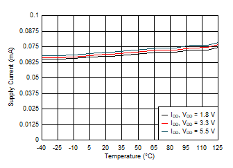
Figure 34. Power-Down Current vs Temperature
DAC53401 DAC43401 SLASES7-Plot-042.gif
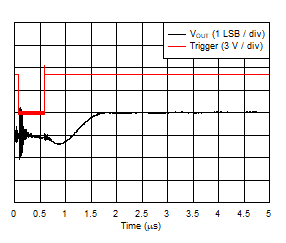
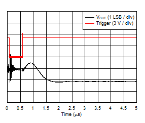
Reference = VDD = 5.5 V, DAC code transition from midscale to midscale + 1 LSB, DAC load = 5kΩ || 200pF
Figure 36. Glitch Impulse, Rising Edge, 1-LSB Step
DAC53401 DAC43401 SLASES7-Plot-045.gif
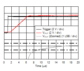
Reference = VDD = 5.5 V, DAC load = 5kΩ || 200pF
Figure 38. Full-Scale Settling Time, Rising Edge
DAC53401 DAC43401 SLASES7-Plot-047.gif
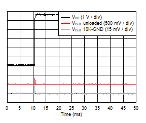
Reference = VDD = 5.5 V
Figure 40. Power-on Glitch
DAC53401 DAC43401 SLASES7-Plot-049.gif
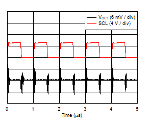
Reference = VDD = 5.5 V, Fast+ mode, DAC at midscale, DAC load = 5kΩ || 200pF
Figure 42. Clock Feedthrough
DAC53401 DAC43401 SLASES7-Plot-051.gif
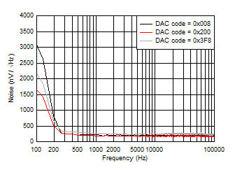
Reference = VDD = 5.5 V
Figure 44. DAC Output Noise Spectral Density
DAC53401 DAC43401 SLASES7-Plot-053.gif
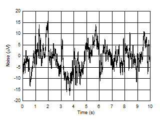
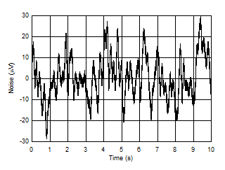
Reference = VDD = 5.5 V, DAC at midscale
Figure 46. DAC Output Noise: 0.1 Hz to 10 Hz
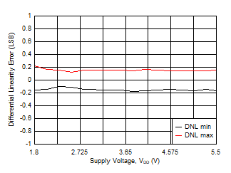
DAC53401 DAC43401 SLASES7-Plot-022.gif
Reference = VDD
Figure 23. Differential Linearity Error vs Supply Voltage
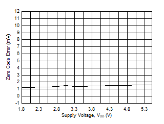
DAC53401 DAC43401 SLASES7-Plot-024.gif
Reference = VDD
Figure 25. Zero-Code Error vs Supply Voltage
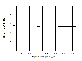
DAC53401 DAC43401 SLASES7-Plot-026.gif
Reference = VDD
Figure 27. Gain Error vs Supply Voltage
DAC53401 DAC43401 SLASES7-Plot-035.gif
VDD = 1.8 V
Figure 29. Supply Current vs Digital Input Code
DAC53401 DAC43401 SLASES7-Plot-037.gif
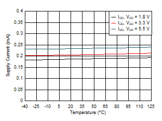
Reference = VDD, DAC at midscale
Figure 31. Supply Current vs Temperature
DAC53401 DAC43401 SLASES7-Plot-039.gif
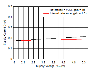
DAC at midscale
Figure 33. Supply Current vs Supply Voltage
DAC53401 DAC43401 SLASES7-Plot-041.gif
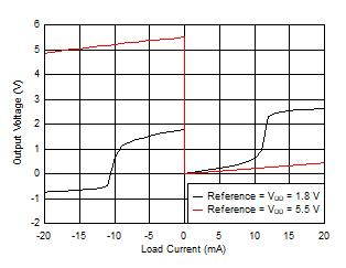
Figure 35. Source and Sink Capability
DAC53401 DAC43401 SLASES7-Plot-044.gif
Reference = VDD = 5.5 V, DAC code transition from midscale to midscale – 1 LSB, DAC load = 5kΩ || 200pF
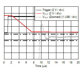
Figure 37. Glitch Impulse, Falling Edge, 1-LSB Step
DAC53401 DAC43401 SLASES7-Plot-046.gif
Reference = VDD = 5.5 V, DAC load = 5kΩ || 200pF
Figure 39. Full-Scale Settling Time, Falling Edge
DAC53401 DAC43401 SLASES7-Plot-048.gif
Reference = VDD = 5.5 V
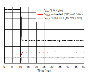
Figure 41. Power-off Glitch
DAC53401 DAC43401 SLASES7-Plot-050.gif
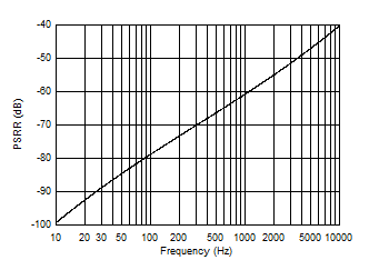
Internal reference (gain = 4x), VDD = 5.25 V + 0.25 VPP, DAC at midscale, DAC load = 5kΩ || 200pF
Figure 43. DAC Output AC PSRR vs Frequency
DAC53401 DAC43401 SLASES7-Plot-052.gif
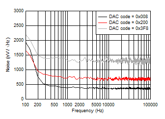
Internal reference (gain = 4x), VDD = 5.5 V
Figure 45. DAC Output Noise Spectral Density
DAC53401 DAC43401 SLASES7-Plot-054.gif
Internal reference (gain = 4x), VDD = 5.5 V, DAC at midscale
Figure 47. DAC Output Noise: 0.1 Hz to 10 Hz