JAJSD57F February 2006 – September 2016 DIX4192
PRODUCTION DATA.
- 1 特長
- 2 アプリケーション
- 3 概要
- 4 改訂履歴
- 5 概要(続き)
- 6 Device Comparison Table
- 7 Pin Configuration and Functions
- 8 Specifications
-
9 Detailed Description
- 9.1 Overview
- 9.2 Functional Block Diagram
- 9.3
Feature Description
- 9.3.1 RESET Operation
- 9.3.2 Master and Reference Clocks
- 9.3.3 Audio Serial Port Operation
- 9.3.4 Overview of the AES3 Digital Audio Interface Protocol
- 9.3.5 Digital Interface Transmitter (DIT) Operation
- 9.3.6 Digital Interface Receiver (DIR) Operation
- 9.3.7 General-Purpose Digital Outputs
- 9.3.8 Interrupt Output
- 9.4 Device Functional Modes
- 9.5 Register Maps
- 10Application and Implementation
- 11Power Supply Recommendations
- 12Layout
- 13デバイスおよびドキュメントのサポート
- 14メカニカル、パッケージ、および注文情報
パッケージ・オプション
メカニカル・データ(パッケージ|ピン)
- PFB|48
サーマルパッド・メカニカル・データ
- PFB|48
発注情報
8 Specifications
8.1 Absolute Maximum Ratings
over operating free-air temperature range (unless otherwise noted)(1)| MIN | MAX | UNIT | ||
|---|---|---|---|---|
| Power supply | VDD18 | –0.3 | 2 | V |
| VDD33 | –0.3 | 4 | ||
| VIO | –0.3 | 4 | ||
| VCC | –0.3 | 4 | ||
| Digital input voltage: digital logic | RXCKI, CPM, CS, CCLK, CDIN, CDOUT, INT, RST, MCLK, BLS, SYNC, BCKA, BCKB, LRCKA, LRCKB, SDINA, SDINB | –0.3 | (VIO + 0.3) | V |
| Line receiver input voltage (per pin) | RX1+, RX1–, RX2+, RX2–, RX3+, RX3–, RX4+, RX4– | (VDD33 + 0.3) | VPP | |
| Input current (all pins except power and ground) | ±10 | mA | ||
| Ambient operating temperature, TA | –40 | 85 | °C | |
| Storage temperature, Tstg | –65 | 150 | °C | |
(1) Stresses beyond those listed under Absolute Maximum Ratings may cause permanent damage to the device. These are stress ratings only, which do not imply functional operation of the device at these or any other conditions beyond those indicated under Recommended Operating Conditions. Exposure to absolute-maximum-rated conditions for extended periods may affect device reliability.
8.2 ESD Ratings
| VALUE | UNIT | |||
|---|---|---|---|---|
| V(ESD) | Electrostatic discharge | Human-body model (HBM), per ANSI/ESDA/JEDEC JS-001(1) | ±2500 | V |
| Charged-device model (CDM), per JEDEC specification JESD22-C101(2) | ±1500 | |||
(1) JEDEC document JEP155 states that 500-V HBM allows safe manufacturing with a standard ESD control process.
(2) JEDEC document JEP157 states that 250-V CDM allows safe manufacturing with a standard ESD control process.
8.3 Recommended Operating Conditions
over operating free-air temperature range (unless otherwise noted)8.4 Thermal Information
| THERMAL METRIC(1) | DIX4192 | UNIT | |
|---|---|---|---|
| PFB (TQFP) | |||
| 48 PINS | |||
| RθJA | Junction-to-ambient thermal resistance | 62.0 | °C/W |
| RθJC(top) | Junction-to-case (top) thermal resistance | 12.8 | °C/W |
| RθJB | Junction-to-board thermal resistance | 27.9 | °C/W |
| ψJT | Junction-to-top characterization parameter | 0.3 | °C/W |
| ψJB | Junction-to-board characterization parameter | 27.6 | °C/W |
(1) For more information about traditional and new thermal metrics, see the Semiconductor and IC Package Thermal Metrics application report.
8.5 Electrical Characteristics
all specifications are at TA = 25°C, VDD18 = 1.8 V, VDD33 = 3.3 V, VIO = 3.3 V, and VCC = 3.3 V (unless otherwise noted)| PARAMETER | TEST CONDITIONS | MIN | TYP | MAX | UNIT | |||
|---|---|---|---|---|---|---|---|---|
| DIGITAL I/O CHARACTERISTICS (ALL I/O PINS EXCEPT LINE RECEIVERS AND LINE DRIVER) | ||||||||
| VIH | High-level input voltage | 0.7 × VIO | VIO | V | ||||
| VIL | Low-level input voltage | 0 | 0.3 × VIO | V | ||||
| IIH | High-level input current | IO = –4 mA, MUTE, SDINA, and SDINB pins | 0.5 | 25 | μA | |||
| IO = –4 mA, all other pins | 0.5 | 10 | ||||||
| IIL | Low-level input current | IO = 4 mA | 0.5 | 10 | μA | |||
| VOH | High-level output voltage | 0.8 × VIO | VIO | V | ||||
| VOL | Low-level output voltage | 0 | 0.2 × VIO | V | ||||
| CIN | Input capacitance | 3 | pF | |||||
| LINE RECEIVER INPUTS (RX1+, RX1–, RX2+, RX2–, RX3+, RX3–, RX4+, RX4–) | ||||||||
| VTH | Differential input sensitivity | Voltage across a given differential input pair | 150 | 200 | mV | |||
| VHY | Input hysteresis | 150 | mV | |||||
| LINE DRIVER OUTPUTS (TX+, TX–) | ||||||||
| VTXO | Differential output voltage | RL = 110 Ω across TX+ and TX– | 5.4 | VPP | ||||
| MASTER CLOCK INPUT | ||||||||
| fMCLK | Master clock input (MCLK) frequency | 1 | 27.7 | MHz | ||||
| fMCLKD | Master clock input (MCLK) duty cycle | 45% | 55% | |||||
| DIGITAL AUDIO INTERFACE RECEIVER (DIR) | ||||||||
| PLL lock range | TA = 25°C | 20 | 216 | kHz | ||||
| fRXCKI | Reference clock input (RXCKI) frequency | 3.5 | 27.7 | MHz | ||||
| fRXCKID | Reference clock input (RXCKI) duty cycle | 45% | 55% | |||||
| fRXCKO | Recovered clock output (RXCKO) frequency | 3.5 | 27.7 | MHz | ||||
| fRXCKOD | Recovered clock output (RXCKO) duty cycle | 45% | 55% | |||||
| Recovered clock output (RXCKO) intrinsic jitter | Measured cycle-to-cycle | 250 | ps RMS | |||||
| DIGITAL AUDIO INTERFACE TRANSMITTER (DIT) | ||||||||
| Intrinsic output jitter | Measured cycle-to-cycle | 200 | ps RMS | |||||
| POWER SUPPLIES | ||||||||
| Supply current: initial startup | All blocks powered down by default | |||||||
| IDD18S | VDD18 = 1.8 V | 10 | μA | |||||
| IDD33S | VDD33 = 3.3 V | 10 | ||||||
| IIOS | VIO = 3.3 V | 300 | ||||||
| ICCS | VCC = 3.3 V | 10 | ||||||
| Supply current: quiescent | All blocks powered up with no clocks applied | |||||||
| IDD18Q | VDD18 = 1.8 V | 2.3 | mA | |||||
| IDD33Q | VDD33 = 3.3 V | 0.6 | ||||||
| IIOQ | VIO = 3.3 V | 0.3 | ||||||
| ICCQ | VCC = 3.3 V | 6.3 | ||||||
| Supply current: dynamic | All blocks powered up, fS = 48 kHz | |||||||
| IDD18D | VDD18 = 1.8 V | 5.1 | mA | |||||
| IDD33D | VDD33 = 3.3 V | 14.1 | ||||||
| IIOD(1) | VIO = 3.3 V | 46 | ||||||
| ICCD | VCC = 3.3 V | 7.4 | ||||||
| Supply current: high sampling rate | All blocks powered up, fS = 192 kHz | |||||||
| IDD18H | VDD18 = 1.8 V | 6.7 | mA | |||||
| IDD33H | VDD33 = 3.3 V | 15 | ||||||
| IIOH(1) | VIO = 3.3 V | 47 | ||||||
| ICCH | VCC = 3.3 V | 7.5 | ||||||
| Total power dissipation: initial startup | All blocks powered down by default | 1 | mW | |||||
| Total power dissipation: quiescent | All blocks powered up with no clocks applied | 28 | mW | |||||
| Total power dissipation: dynamic | All blocks powered up, fS = 48 kHz | 233 | mW | |||||
| Total power dissipation: high sampling rate | All blocks powered up, fS = 192 kHz | 242 | mW | |||||
(1) The typical VIO supply current is measured using the DIX4192EVM evaluation module with loading from the DAIMB motherboard circuitry. VIO supply current is dependent upon the loading on the logic output pins.
8.6 Timing Requirements
| MIN | NOM | MAX | UNIT | ||
|---|---|---|---|---|---|
| AUDIO SERIAL PORTS (PORT A AND PORT B) | |||||
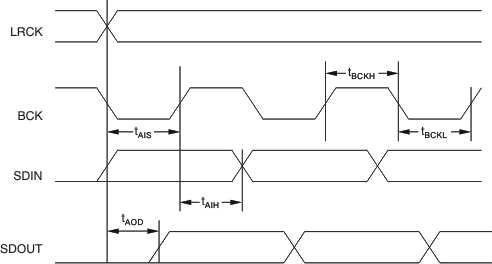
| fLRCK | LRCK clock frequency | 0 | 216 | kHz | |
| tLRCKD | LRCK clock duty cycle | 50% | |||
| fBCK | BCK clock frequency | 0 | 13.824 | MHz | |
| tBCKH | BCK high pulse duration | 10 | ns | ||
| tBCKL | BCK low pulse duration | 10 | ns | ||
| tAIS | Audio data Input (SDIN) set-up time | 10 | ns | ||
| tAISH | Audio data input (SDIN) hold time | 10 | ns | ||
| tADD | Audio data output (SDOUT) delay | 10 | ns | ||
| HOST INTERFACE: SPI MODE | |||||
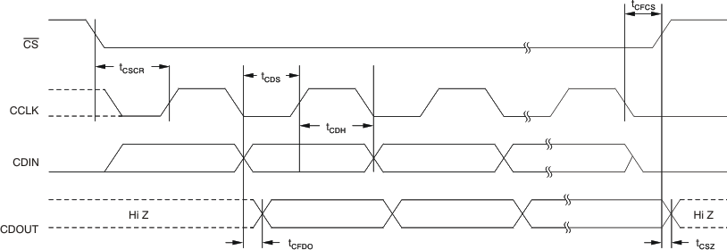
| fCCLK | Serial clock (CCLK) frequency | 0 | 40 | MHz | |
| tCSCR | CS falling to CCLK rising | 8 | ns | ||
| tCFCS | CCLK falling to CS rising | 7 | ns | ||
| tCDS | CDIN data set-up time | 7 | ns | ||
| tCDH | CDIN data hold time | 6 | ns | ||
| tCFDO | CCLK falling to CDOUT data valid | 3 | ns | ||
| tCSZ | CS rising to CDOUT high-impedance | 3 | ns | ||
| HOST INTERFACE: I2C STANDARD MODE(1) | |||||
| fSCL | SCL clock frequency | 0 | 100 | kHz | |
| tHDSTA | Hold time repeated START condition | 4 | μs | ||
| tLOW | Low period of SCL clock | 4.7 | μs | ||
| tHIGH | High period of SCL clock | 4 | μs | ||
| tSUSTA | Set-up time repeated START condition | 4.7 | μs | ||
| tHDDAT | Data hold time | 0(2) | 3.45(4) | μs | |
| tSUDAT | Data set-up time | 250 | ns | ||
| tR | Rise time for both SDA and SDL | 1000 | ns | ||
| tF | Fall time for both SDA and SDL | 300 | ns | ||
| tSUSTO | Set-up time for STOP condition | 4 | μs | ||
| tBUF | Bus free time between START and STOP | 4.7 | μs | ||
| CB | Capacitive load for each bus line | 400 | pF | ||
| VNL | Noise margin at low level (including hysteresis) | 0.1 × VIO | V | ||
| VNH | Noise margin at high level (including hysteresis) | 0.2 × VIO | V | ||
| HOST INTERFACE: I2C FAST MODE(1) | |||||
| fSCL | SCL clock frequency | 0 | 400 | kHz | |
| tHDSTA | Hold time repeated START condition | 0.6 | μs | ||
| tLOW | Low period of SCL clock | 1.3 | μs | ||
| tHIGH | High period of SCL clock | 0.6 | μs | ||
| tSUSTA | Set-up time repeated START condition | 0.6 | μs | ||
| tHDDAT | Data hold time | 0(2) | 0.9(4) | μs | |
| tSUDAT | Data set-up time | 100(5) | ns | ||
| tR | Rise time for both SDA and SDL | 20 + 0.2CB (3) | 300 | ns | |
| tF | Fall time for both SDA and SDL | 20 + 0.2CB (3) | 300 | ns | |
| tSUSTO | Set-up time for STOP condition | 0.6 | μs | ||
| tBUF | Bus free time between START and STOP | 1.3 | μs | ||
| tSP | Spike pulse duration suppressed by input filter | 0 | 50 | ns | |
| CB | Capacitive load for each bus Line | 400 | pF | ||
| VNL | Noise margin at low level (including hysteresis) | 0.1 × VIO | V | ||
| VNH | Noise margin at high level (including hysteresis) | 0.2 × VIO | V | ||
(1) All values referred to the VIH minimum and VIL maximum levels listed in the Digital I/O Characteristics section of this table.
(2) A device must internally provide a hold time of at least 300 ns for the SDA signal (referred to the VIH minimum input level) to bridge the undefined region of the falling edge of SCL.
(3) CB is defined as the total capacitance of one bus line in picofarads (pF). If mixed with High-Speed mode devices, faster fall times are allowed.
(4) The maximum tHDDAT has only to be met if the device does not stretch the Low period (tLOW) of the SCL signal.
(5) A Fast mode I2C bus device can be used in a Standard mode I2C bus system, but the requirement that tSUDAT be 250 ns (minimum) must then be met. For the DIX4192, this condition is automatically the case, because the device does not stretch the Low period of the SCL signal.
 Figure 1. Audio Serial Port Timing
 Figure 2. SPI Timing
 Figure 3. I2C Standard and Fast Mode Timing
8.7 Typical Characteristics

