SLVSB18H March 2012 – August 2016 DRV8835
PRODUCTION DATA.
- 1 Features
- 2 Applications
- 3 Description
- 4 Revision History
- 5 Pin Configuration and Functions
- 6 Specifications
- 7 Detailed Description
- 8 Application and Implementation
- 9 Power Supply Recommendations
- 10Layout
- 11Device and Documentation Support
- 12Mechanical, Packaging, and Orderable Information
パッケージ・オプション
メカニカル・データ(パッケージ|ピン)
- DSS|12
サーマルパッド・メカニカル・データ
- DSS|12
発注情報
8 Application and Implementation
NOTE
Information in the following applications sections is not part of the TI component specification, and TI does not warrant its accuracy or completeness. TI’s customers are responsible for determining suitability of components for their purposes. Customers should validate and test their design implementation to confirm system functionality.
8.1 Application Information
The DRV8835 is used in one or two motor control applications. Configure the DRV8835 in parallel to provide double the current to one motor. The following design procedure can be used to configure the DRV8835 in a brushed motor application.
8.2 Typical Application
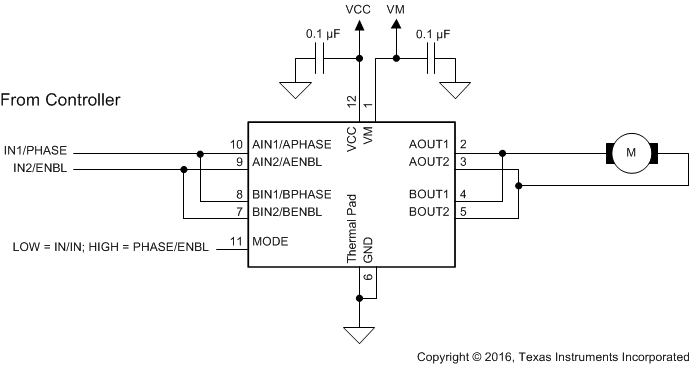
The two H-bridges in the DRV8835 connect in parallel for double the current of a single H-bridge. Figure 6 shows the connections.
8.2.1 Design Requirements
Table 5 lists the design requirements.
Table 5. Design Requirements
| DESIGN PARAMETER | REFERENCE | VALUE |
|---|---|---|
| Motor voltage | VCC | 4 V |
| Motor RMS current | IRMS | 0.3 A |
| Motor startup current | ISTART | 0.6 A |
| Motor current trip point | ILIMIT | 0.5 A |
8.2.2 Detailed Design Procedure
8.2.2.1 Motor Voltage
The appropriate motor voltage depends on the ratings of the motor selected and the desired RPM. A higher voltage spins a brushed DC motor faster with the same PWM duty cycle applied to the power FETs. A higher voltage also increases the rate of current change through the inductive motor windings.
8.2.2.2 Lower-Power Operation
When entering sleep mode, TI recommends setting all inputs as a logic low to minimize system power.
8.2.3 Application Curve
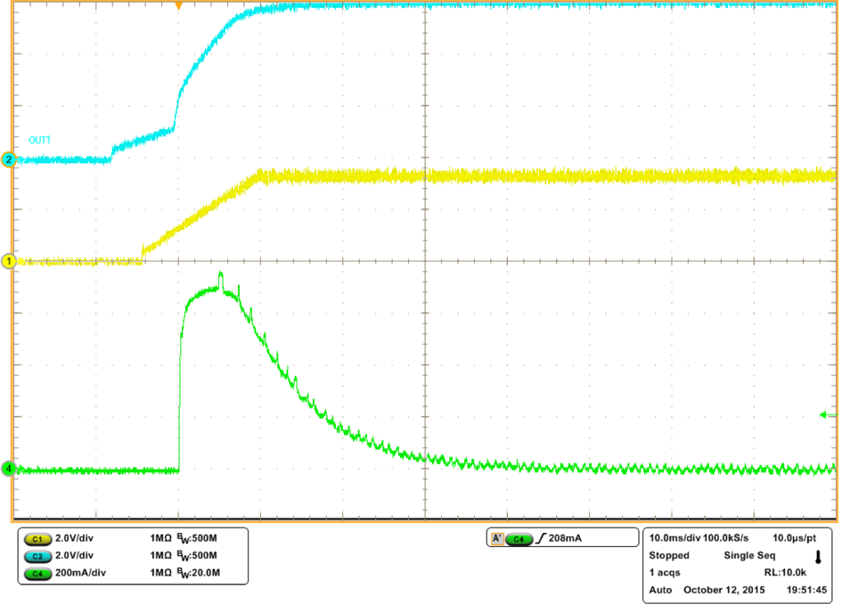
The following scope captures motor startup as VCC ramps from 0 V to 6 V. Channel 1 is VCC, Channel 2 is VM, and Channel 4 is the motor current of an unloaded motor during startup. The motor used is a NMB Technologies Corporation, PPN7PA12C1. As VCC and VM ramp, the current in the motor increases until the motor speed builds up. The motor current then reduces for normal operation.
Inputs are set as follows:
- Mode: IN/IN
- AIN1: High
- AIN2: Low

| Channel 1: VM | IN1 = Logic High | |
| Channel 2: VCC | IN2 = Logic Low | Motor used: NMB Technologies Corporation, PPN7PA12C1 |
| Channel 4: Motor current |
