SLVSD18C June 2015 – August 2017 DRV8880
PRODUCTION DATA.
- 1 Features
- 2 Applications
- 3 Description
- 4 Revision History
- 5 Pin Configuration and Functions
- 6 Specifications
-
7 Detailed Description
- 7.1 Overview
- 7.2 Functional Block Diagram
- 7.3
Feature Description
- 7.3.1 Stepper Motor Driver Current Ratings
- 7.3.2 PWM Motor Drivers
- 7.3.3 Microstepping Indexer
- 7.3.4 Current Regulation
- 7.3.5
Decay Modes
- 7.3.5.1 Mode 1: Slow Decay for Increasing and Decreasing Current
- 7.3.5.2 Mode 2: Slow Decay for Increasing Current, Mixed Decay for Decreasing current
- 7.3.5.3 Mode 3: Mixed Decay for Increasing and Decreasing Current
- 7.3.5.4 Mode 4: Slow Decay for Increasing Current, Fast Decay for Decreasing current
- 7.3.5.5 Mode 5: Fast Decay for Increasing and Decreasing Current
- 7.3.6 Smart Tune
- 7.3.7 Adaptive Blanking Time
- 7.3.8 Charge Pump
- 7.3.9 LDO Voltage Regulator
- 7.3.10 Logic and Tri-Level Pin Diagrams
- 7.3.11 Power Supplies and Input Pins
- 7.3.12 Protection Circuits
- 7.3.13 VM UVLO (UVLO2)
- 7.3.14 Logic Undervoltage (UVLO1)
- 7.3.15 VCP Undervoltage Lockout (CPUV)
- 7.3.16 Thermal Shutdown (TSD)
- 7.3.17 Overcurrent Protection (OCP)
- 7.4 Device Functional Modes
- 8 Application and Implementation
- 9 Power Supply Recommendations
- 10Layout
- 11Device and Documentation Support
- 12Mechanical, Packaging, and Orderable Information
パッケージ・オプション
デバイスごとのパッケージ図は、PDF版データシートをご参照ください。
メカニカル・データ(パッケージ|ピン)
- RHR|28
- PWP|28
サーマルパッド・メカニカル・データ
発注情報
10 Layout
10.1 Layout Guidelines
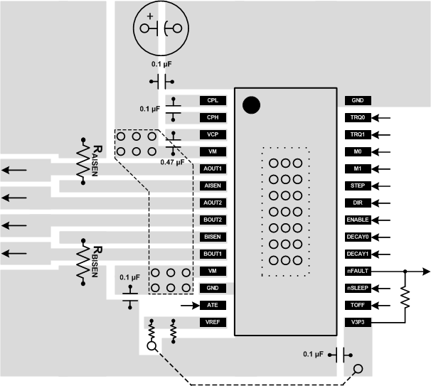
Each VM terminal must be bypassed to GND using a low-ESR ceramic bypass capacitors with recommended values of 0.1 μF rated for VM. These capacitors should be placed as close to the VM pins as possible with a thick trace or ground plane connection to the device GND pin.
The VM pin must be bypassed to ground using a bulk capacitor rated for VM. This component may be an electrolytic.
A low-ESR ceramic capacitor must be placed in between the CPL and CPH pins. A value of 0.1 μF rated for VM is recommended. Place this component as close to the pins as possible.
A low-ESR ceramic capacitor must be placed in between the VM and VCP pins. A value of 0.47 μF rated for 16 V is recommended. Place this component as close to the pins as possible.
Bypass V3P3 to ground with a ceramic capacitor rated 6.3 V. Place this bypassing capacitor as close to the pin as possible.
The current sense resistors should be placed as close as possible to the device pins in order to minimize trace inductance between the pin and resistor.
10.2 Layout Example
 Figure 36. Layout Recommendation