JAJSI42D March 2016 – October 2019 DS250DF410
PRODUCTION DATA.
- 1 特長
- 2 アプリケーション
- 3 概要
- 4 改訂履歴
- 5 概要 (続き)
- 6 Pin Configuration and Functions
-
7 Specifications
- 7.1 Absolute Maximum Ratings
- 7.2 ESD Ratings
- 7.3 Recommended Operating Conditions
- 7.4 Thermal Information
- 7.5 Electrical Characteristics
- 7.6 Timing Requirements, Retimer Jitter Specifications
- 7.7 Timing Requirements, Retimer Specifications
- 7.8 Timing Requirements, Recommended Calibration Clock Specifications
- 7.9 Recommended SMBus Switching Characteristics (Slave Mode)
- 7.10 Recommended SMBus Switching Characteristics (Master Mode)
- 7.11 Recommended JTAG Switching Characteristics
- 7.12 Typical Characteristics
-
8 Detailed Description
- 8.1 Overview
- 8.2 Functional Block Diagram
- 8.3
Feature Description
- 8.3.1 Device Data Path Operation
- 8.3.2 Signal Detect
- 8.3.3 Continuous Time Linear Equalizer (CTLE)
- 8.3.4 Variable Gain Amplifier (VGA)
- 8.3.5 Cross-Point Switch
- 8.3.6 Decision Feedback Equalizer (DFE)
- 8.3.7 Clock and Data Recovery (CDR)
- 8.3.8 Calibration Clock
- 8.3.9 Differential Driver with FIR Filter
- 8.3.10 Debug Features
- 8.3.11 Interrupt Signals
- 8.3.12 JTAG Boundary Scan
- 8.4 Device Functional Modes
- 8.5 Programming
- 8.6 Register Maps
- 9 Application and Implementation
- 10Power Supply Recommendations
- 11Layout
- 12デバイスおよびドキュメントのサポート
- 13メカニカル、パッケージ、および注文情報
9.2.1 Front-Port Jitter Cleaning Applications
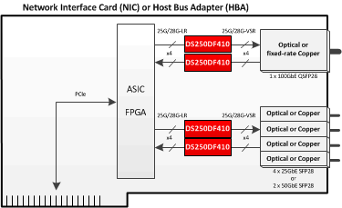
The DS250DF410 has strong equalization capabilities that allow it to equalize insertion loss, reduce jitter, and extend the reach of front-port interfaces. A single DS250DF410 can be used to support all four egress channels for a 100GbE port. Another DS250DF410 can be used to support all four ingress channels for the same 100GbE ports. Alternatively, a single DS250DF410 can be used to support all egress channels for four 25GbE ports, and another DS250DF410 can be used to support all four ingress channels for the same four 25GbE ports.
For applications which require IEEE802.3 100GBASE-CR4 or 25GBASE-CR auto-negotiation and link training, a linear repeater device such as the DS280BR810 (or similar) is recommended.
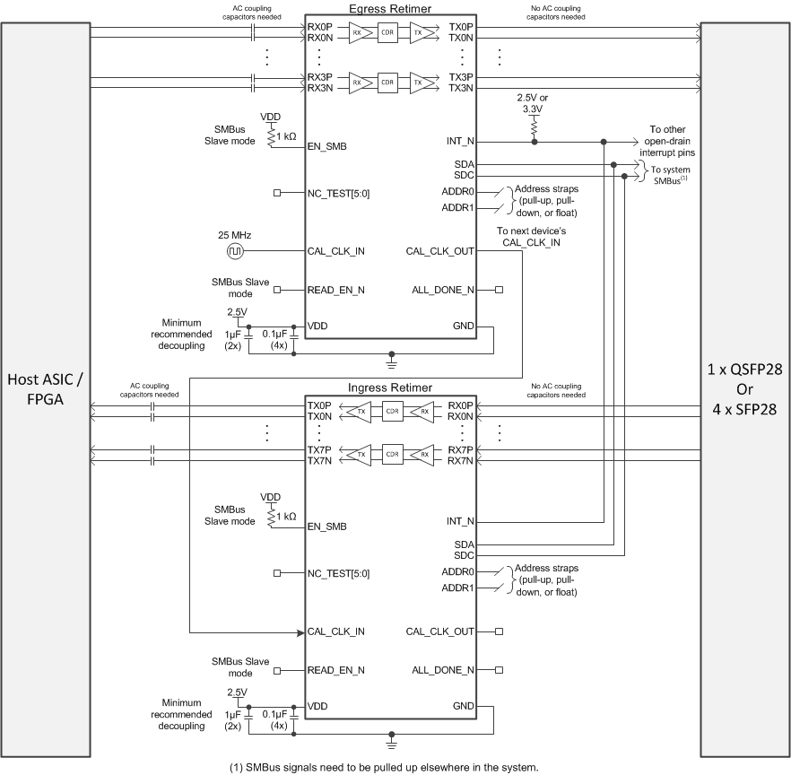
Figure 16 illustrates this configuration, and Figure 17 shows an example simplified schematic for a typical front-port application.
 Figure 16. Front-Port Application Block Diagram
  Figure 17. Front-Port Application Schematic