SNOSCY5B August 2014 – April 2015 FDC1004
PRODUCTION DATA.
- 1 Features
- 2 Applications
- 3 Description
- 4 Typical Application
- 5 Revision History
- 6 Pin Configuration and Functions
- 7 Specifications
- 8 Detailed Description
- 9 Applications and Implementation
- 10Power Supply Recommendations
- 11Layout
- 12Device and Documentation Support
- 13Mechanical, Packaging, and Orderable Information
パッケージ・オプション
メカニカル・データ(パッケージ|ピン)
サーマルパッド・メカニカル・データ
- DSC|10
発注情報
7 Specifications
7.1 Absolute Maximum Ratings(1)
| MIN | MAX | UNIT | ||
|---|---|---|---|---|
| Input voltage | VDD | –0.3 | 6 | V |
| SCL, SDA | –0.3 | 6 | V | |
| at any other pin | –0.3 | VDD+0.3 | V | |
| Input current | at any pin | 3 | mA | |
| Junction temperature(2) | 150 | °C | ||
| Storage temperature | TSTG | –65 | 150 | °C |
(1) Stresses beyond those listed under Absolute Maximum Ratings may cause permanent damage to the device. These are stress ratings only, which do not imply functional operation of the device at these or any other conditions beyond those indicated under Recommended Operating Conditions. Exposure to absolute-maximum-rated conditions for extended periods may affect device reliability.
(2) The maximum power dissipation is a function of TJ(MAX), RθJA, and the ambient temperature, TA. The maximum allowable power dissipation at any ambient temperature is PDMAX = (TJ(MAX) - TA)/ RθJA. All numbers apply for packages soldered directly onto a PC board.
7.2 ESD Ratings
| VALUE | UNIT | |||
|---|---|---|---|---|
| V(ESD) | Electrostatic discharge(1) | Human body model (HBM), per ANSI/ESDA/JEDEC JS-001, all pins(2) | ±1000 | V |
| Charged device model (CDM), per JEDEC specification -500 500 JESD22-C101, all pins(3) | ±250 | |||
(1) Electrostatic discharge (ESD) to measure device sensitivity and immunity to damage caused by assembly line electrostatic discharges in to the device.
(2) Level listed above is the passing level per ANSI, ESDA, and JEDEC JS-001. JEDEC document JEP155 states that 500-V HBM allows safe manufacturing with a standard ESD control process.
(3) Level listed above is the passing level per EIA-JEDEC JESD22-C101. JEDEC document JEP157 states that 250-V CDM allows safe manufacturing with a standard ESD control process.
7.3 Recommended Operating Conditions
Over operating temperature range (unless otherwise noted)| MIN | NOM | MAX | UNIT | ||
|---|---|---|---|---|---|
| Supply voltage (VDD-GND) | 3 | 3.3 | 3.6 | V | |
| Temperature | –40 | 125 | °C | ||
7.4 Thermal Information
| THERMAL METRIC(1) | FDC1004 | UNIT | ||
|---|---|---|---|---|
| WSON (DSC) | VSSOP (DGS) | |||
| 10 PINS | ||||
| RθJA | Junction-to-ambient thermal resistance | 46.8 | 46.8 | °C/W |
| RθJC | Junction-to-case(top) thermal resistance | 46.7 | 48.7 | °C/W |
| RθJB | Junction-to-board thermal resistance | 21.5 | 70.6 | °C/W |
(1) For more information about traditional and new thermal metrics, see the IC Package Thermal Metrics application report, SPRA953.
7.5 Electrical Characteristics(1)
Over recommended operating temperature range, VDD = 3.3 V, for TA = 25°C (unless otherwise noted).| PARAMETER | TEST CONDITION | MIN(2) | TYP(3) | MAX(2) | UNIT | |
|---|---|---|---|---|---|---|
| POWER SUPPLY | ||||||
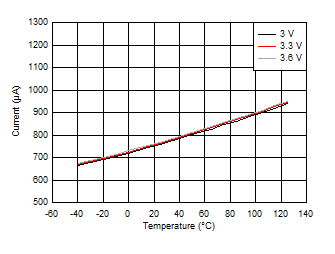
| IDD | Supply current | Conversion mode; Digital input to VDD or GND | 750 | 950 | µA | |
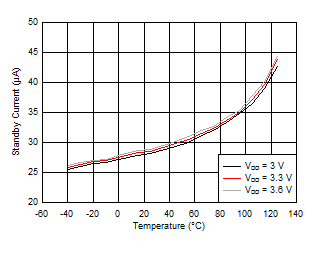
| Standby; Digital input to VDD or GND | 29 | 70 | µA | |||
| CAPACITIVE INPUT | ||||||
| ICR | Input conversion range | ±15 | pF | |||
| COMAX | Max input offset capacitance | per channel, Series resistance at CINn n=1.4 = 0 Ω | 100 | pF | ||
| RES | Effective resolution (4) | Sample rate = 100S/s (5) | 16 | bit | ||
| EON | Output noise | Sample rate = 100S/s (5) | 33.2 | aF/√Hz | ||
| ERR | Absolute error | after offset calibration | ±6 | fF | ||
| TcCOFF | Offset deviation over temperature | -40°C < T < 125°C | 46 | fF | ||
| GERR | Gain error | 0.2 | % | |||
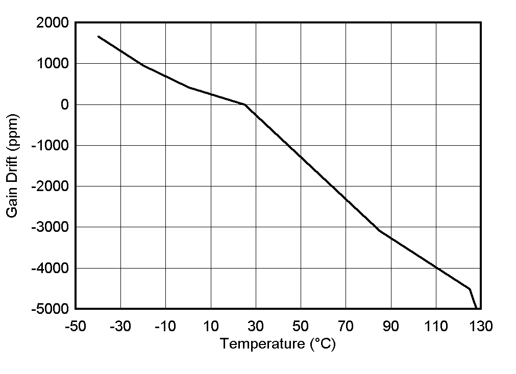
| tcG | Gain drift vs. temperature | -40°C < T < 125°C | -37.5 | ppm/°C | ||
| PSRR | DC power supply rejection | 3 V < VDD < 3.6 V, single-ended mode (channel vs GND) | 13.6 | fF/V | ||
| CAPDAC | ||||||
| FRCAPDAC | Full-scale range | 96.9 | pF | |||
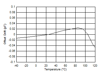
| TcCOFFCAPDAC | Offset drift vs. temperature | -40°C < T < 125°C | 30 | fF | ||
| EXCITATION | ||||||
| ƒ | Frequency | 25 | kHz | |||
| VAC | AC voltage across capacitance | 2.4 | Vpp | |||
| VDC | Average DC voltage across capacitance | 1.2 | V | |||
| SHIELD | ||||||
| DRV | Driver capability | ƒ = 25 kHz, SHLDn to GND, n = 1,2 | 400 | pF | ||
(1) Electrical Characteristics Table values apply only for factory testing conditions at the temperature indicated. Factor testing conditions result in very limited self-heating of the device such that TJ=TA. No guarantee of parametric performance is indicated in the electrical tables under conditions of internal self-heating where TJ>TA. Absolute Maximum Ratings indicate junction temperature limits beyond which the device may be permanently degraded, either mechanically or electrically.
(2) Limits are ensured by testing, design, or statistical analysis at 25Degree C. Limits over the operating temperature range are ensured through correlations using statistical quality control (SQC) method.
(3) Typical values represent the most likely parametric norm as determined at the time of characterization. Actual typical values may vary over time and will also depend on the application and configuration. The typical values are not tested and are not guaranteed on shipped production material.
(4) Effective resolution is the ratio of converter full scale range to RMS measurement noise.
(5) No external capacitance connected.
7.6 I2C Interface Voltage Level
Over recommended operating free-air temperature range, VDD = 3.3 V, for TA = TJ = 25°C (unless otherwise noted).| PARAMETER | TEST CONDITIONS | MIN | TYP | MAX | UNIT | |
|---|---|---|---|---|---|---|
| VIH | Input high voltage | 0.7*VDD | V | |||
| VIL | Input low voltage | 0.3*VDD | V | |||
| VOL | Output low voltage | Sink current 3 mA | 0.4 | V | ||
| HYS | Hysteresis (1) | 0.1*VDD | V | |||
(1) This parameter is specified by design and/or characterization and is not tested in production.
7.7 I2C Interface Timing
Over recommended operating free-air temperature range, VDD = 3.3 V, for TA = TJ = 25°C (unless otherwise noted).| PARAMETER | TEST CONDITIONS | MIN | TYP | MAX | UNIT | |
|---|---|---|---|---|---|---|
| fSCL | Clock frequency(1) | 10 | 400 | kHz | ||
| tLOW | Clock low time(1) | 1.3 | µs | |||
| tHIGH | Clock high time(1) | 0.6 | µs | |||
| tHD;STA | Hold time (repeated) START condition(1) | After this period, the first clock pulse is generated | 0.6 | µs | ||
| tSU;STA | Set-up time for a repeated START condition(1) | 0.6 | µs | |||
| tHD;DAT | Data hold time(1)(2) | 0 | ns | |||
| tSU;DAT | Data setup time(1) | 100 | ns | |||
| tf | SDA fall time(1) | IL ≤ 3mA; CL ≤ 400pF | 300 | ns | ||
| tSU;STO | Set-up time for STOP condition(1) | 0.6 | µs | |||
| tBUF | Bus free time between a STOP and START condition(1) | 1.3 | µs | |||
| tVD;DAT | Data valid time(1) | 0.9 | ns | |||
| tVD;ACK | Data valid acknowledge time(1) | 0.9 | ns | |||
| tSP | Pulse width of spikes that must be suppressed by the input filter(1) | 50 | ns | |||
(1) This parameter is specified by design and/or characterization and is not tested in production.
(2) The FDC1004 provides an internal 300 ns minimum hold time to bridge the undefined region of the falling edge of SCL.
 Figure 1. I2C Timing
7.8 Typical Characteristics
