SLASE74F May 2015 – September 2016 HD3SS3212
PRODUCTION DATA.
- 1 Features
- 2 Applications
- 3 Description
- 4 Revision History
- 5 Device Comparison Table
- 6 Pin Configuration and Functions
- 7 Specifications
- 8 Parameter Measurement Information
- 9 Detailed Description
- 10Application and Implementation
- 11Power Supply Recommendations
- 12Layout
- 13Device and Documentation Support
- 14Mechanical, Packaging, and Orderable Information
パッケージ・オプション
デバイスごとのパッケージ図は、PDF版データシートをご参照ください。
メカニカル・データ(パッケージ|ピン)
- RKS|20
サーマルパッド・メカニカル・データ
発注情報
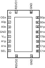
6 Pin Configuration and Functions
RKS Package
20-Pin VQFN
Top View

Pin Functions
| PIN | TYPE(1) | DESCRIPTION | |
|---|---|---|---|
| NAME | NO. | ||
| VCC | 6 | P | 3.3-V power |
| OEn | 2 | I | Active-low chip enable L: Normal operation H: Shutdown |
| A0p | 3 | I/O | Port A, channel 0, high-speed positive signal |
| A0n | 4 | I/O | Port A, channel 0, high-speed negative signal |
| GND | 5, 11, 20 | G | Ground |
| A1p | 7 | I/O | Port A, channel 1, high-speed positive signal |
| A1n | 8 | I/O | Port A, channel 1, high-speed negative signal |
| SEL | 9 | I | Port select pin. L: Port A to Port B H: Port A to Port C |
| C1n | 12 | I/O | Port C, channel 1, high-speed negative signal (connector side) |
| C1p | 13 | I/O | Port C, channel 1, high-speed positive signal (connector side) |
| C0n | 14 | I/O | Port C, channel 0, high-speed negative signal (connector side) |
| C0p | 15 | I/O | Port C, channel 0, high-speed positive signal (connector side) |
| B1n | 16 | I/O | Port B, channel 1, high-speed negative signal (connector side) |
| B1p | 17 | I/O | Port B, channel 1, high-speed positive signal (connector side) |
| B0n | 18 | I/O | Port B, channel 0, high-speed negative signal (connector side) |
| B0p | 19 | I/O | Port B, channel 0, high-speed positive signal (connector side) |
| RSVD1 | 1 | O | Can be left not connected or can be fed to VCC |
| RSVD2 | 10 | O | |
(1) The high-speed data ports incorporate 20-kΩ pulldown resistors that are switched in when a port is not selected and switched out when the port is selected.