JAJSCN1E December   1999  – December 2017 INA138 , INA168

PRODUCTION DATA.  

  1. 特長
  2. アプリケーション
  3. 概要
    1.     Device Images
      1.      代表的なアプリケーション回路
  4. 改訂履歴
  5. Pin Configuration and Functions
    1.     Pin Functions
  6. Specifications
    1. 6.1 Absolute Maximum Ratings
    2. 6.2 ESD Ratings
    3. 6.3 Recommended Operating Conditions
    4. 6.4 Thermal Information
    5. 6.5 Electrical Characteristics
    6. 6.6 Typical Characteristics
  7. Detailed Description
    1. 7.1 Overview
    2. 7.2 Functional Block Diagram
    3. 7.3 Feature Description
      1. 7.3.1 Output Voltage Range
      2. 7.3.2 Bandwidth
    4. 7.4 Device Functional Modes
  8. Application and Implementation
    1. 8.1 Application Information
      1. 8.1.1 Operation
    2. 8.2 Typical Applications
      1. 8.2.1 Buffering Output to Drive an ADC
        1. 8.2.1.1 Design Requirements
        2. 8.2.1.2 Detailed Design Procedure
          1. 8.2.1.2.1 Selecting the Shunt Resistor and RL
        3. 8.2.1.3 Application Curve
      2. 8.2.2 Output Filter
        1. 8.2.2.1 Design Requirements
        2. 8.2.2.2 Detailed Design Procedure
        3. 8.2.2.3 Application Curve
      3. 8.2.3 Offsetting the Output Voltage
      4. 8.2.4 Bipolar Current Measurement
      5. 8.2.5 Bipolar Current Measurement Using Differential Input of ADC
      6. 8.2.6 Multiplexed Measurement Using Logic Signal for Power
  9. Power Supply Recommendations
  10. 10Layout
    1. 10.1 Layout Guidelines
    2. 10.2 Layout Example
  11. 11デバイスおよびドキュメントのサポート
    1. 11.1 ドキュメントのサポート
      1. 11.1.1 関連資料
    2. 11.2 関連リンク
    3. 11.3 ドキュメントの更新通知を受け取る方法
    4. 11.4 コミュニティ・リソース
    5. 11.5 商標
    6. 11.6 静電気放電に関する注意事項
    7. 11.7 Glossary
  12. 12メカニカル、パッケージ、および注文情報

パッケージ・オプション

メカニカル・データ(パッケージ|ピン)
サーマルパッド・メカニカル・データ
発注情報

Operation

Figure 9 illustrates the basic circuit diagram for both the INA138 and INA168 devices. Load current IS is drawn from supply VS through shunt resistor RS. The voltage drop in shunt resistor VS is forced across RG1 by the internal op amp, causing current to flow into the collector of Q1. External resistor RL converts the output current to a voltage, VOUT, at the OUT pin. The transfer function for the INA138 device is:

Equation 3. IO = gm(VIN+ – VIN–)

where gm = 200 µA/V.

In the circuit of Figure 9, the input voltage, (VIN+ – VIN–), is equal to IS × RS and the output voltage, VOUT, is equal to IO × RL. The transconductance, gm, of the INA138 device is 200 µA/V. The complete transfer function for the current measurement amplifier in this application is:

Equation 4. VOUT = (IS) (RS) (200 µA/V) (RL)

The maximum differential input voltage for accurate measurements is 0.5 V, which produces a 100-µA output current. A differential input voltage of up to 2 V will not cause damage. Differential measurements (pins 3 and 4) must be unipolar with a more-positive voltage applied to pin 3. If a more-negative voltage is applied to pin 3, the output current, IO, will be zero, but it will not cause damage.
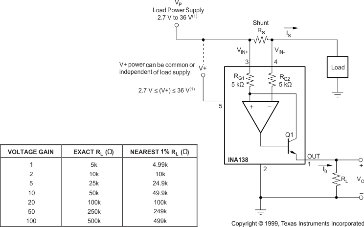
INA138 INA168 basic_circuit_connections_sbos122.gif
Maximum VP and V+ voltage is 60 V with INA168.
Figure 9. Basic Circuit Connections