JAJSCN1E December 1999 – December 2017 INA138 , INA168
PRODUCTION DATA.
- 1 特長
- 2 アプリケーション
- 3 概要
- 4 改訂履歴
- 5 Pin Configuration and Functions
- 6 Specifications
- 7 Detailed Description
-
8 Application and Implementation
- 8.1 Application Information
- 8.2 Typical Applications
- 9 Power Supply Recommendations
- 10Layout
- 11デバイスおよびドキュメントのサポート
- 12メカニカル、パッケージ、および注文情報
8.2.3 Offsetting the Output Voltage
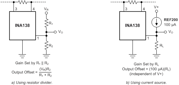
For many applications using only a single power supply it may be required to level shift the output voltage away from ground when there is no load current flowing in the shunt resistor. Level shifting the output of the INA1x8 devices is easily accomplished by one of two simple methods shown in Figure 14. The method on the left hand side of Figure 14 illustrates a simple voltage divider method. This method is useful for applications that require the output of the INA1x8 devices to remain centered with respect to the power supply at zero load current through the shunt resistor. Using this method the gain is determine by the parallel combination of R1 and R2 while the output offset is determined by the voltage divider ratio R1 and R2. For applications that may require a fixed value of output offset, independent of the power supply voltage, the current source method shown on the right-hand side of Figure 14 is recommended. With this method a REF200 constant current source is used to generate a constant output offset. Using his method the gain is determined by RL and the offset is determined by the product of the value of the current source and RL.
 Figure 14. Offsetting the Output Voltage