JAJSH88A April   2019  – June 2019 INA818

PRODUCTION DATA.  

  1. 特長
  2. アプリケーション
  3. 概要
    1.     Device Images
      1.      INA818 の簡略化された内部回路図
      2.      入力段のオフセット電圧ドリフトの代表的な分布
  4. 改訂履歴
  5. Device Comparison Table
  6. Pin Configuration and Functions
    1.     Pin Functions
  7. Specifications
    1. 7.1 Absolute Maximum Ratings
    2. 7.2 ESD Ratings
    3. 7.3 Recommended Operating Conditions
    4. 7.4 Thermal Information
    5. 7.5 Electrical Characteristics
    6. 7.6 Typical Characteristics: Table of Graphs
    7. 7.7 Typical Characteristics
  8. Detailed Description
    1. 8.1 Overview
    2. 8.2 Functional Block Diagram
    3. 8.3 Feature Description
      1. 8.3.1 Setting the Gain
        1. 8.3.1.1 Gain Drift
      2. 8.3.2 EMI Rejection
      3. 8.3.3 Input Common-Mode Range
      4. 8.3.4 Input Protection
      5. 8.3.5 Operating Voltage
      6. 8.3.6 Error Sources
    4. 8.4 Device Functional Modes
  9. Application and Implementation
    1. 9.1 Application Information
      1. 9.1.1 Reference Pin
      2. 9.1.2 Input Bias Current Return Path
    2. 9.2 Typical Applications
      1. 9.2.1 Three-Pin Programmable Logic Controller (PLC)
        1. 9.2.1.1 Design Requirements
        2. 9.2.1.2 Detailed Design Procedure
        3. 9.2.1.3 Application Curves
      2. 9.2.2 Resistance Temperature Detector Interface
  10. 10Power Supply Recommendations
  11. 11Layout
    1. 11.1 Layout Guidelines
    2. 11.2 Layout Example
  12. 12デバイスおよびドキュメントのサポート
    1. 12.1 ドキュメントのサポート
      1. 12.1.1 関連資料
    2. 12.2 ドキュメントの更新通知を受け取る方法
    3. 12.3 コミュニティ・リソース
    4. 12.4 商標
    5. 12.5 静電気放電に関する注意事項
    6. 12.6 Glossary
  13. 13メカニカル、パッケージ、および注文情報

パッケージ・オプション

メカニカル・データ(パッケージ|ピン)
サーマルパッド・メカニカル・データ
発注情報

Input Protection

The inputs of the INA818 device are individually protected for voltages up to ±60 V. For example, a condition of –60 V on one input and +60 V on the other input does not cause damage. Internal circuitry on each input provides low series impedance under normal signal conditions. If the input is overloaded, the protection circuitry limits the input current to a value of approximately 8 mA.
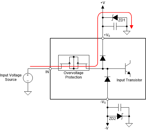
INA818 ai_D004_SBOS792.gifFigure 62. Input Current Path During an Overvoltage Condition

During an input overvoltage condition, current flows through the input protection diodes into the power supplies; see Figure 62. If the power supplies are unable to sink current, then Zener diode clamps (ZD1 and ZD2 in Figure 62) must be placed on the power supplies to provide a current pathway to ground. Figure 63 shows the input current for input voltages from –50 V to +50 V when the INA818 is powered by ±15-V supplies.
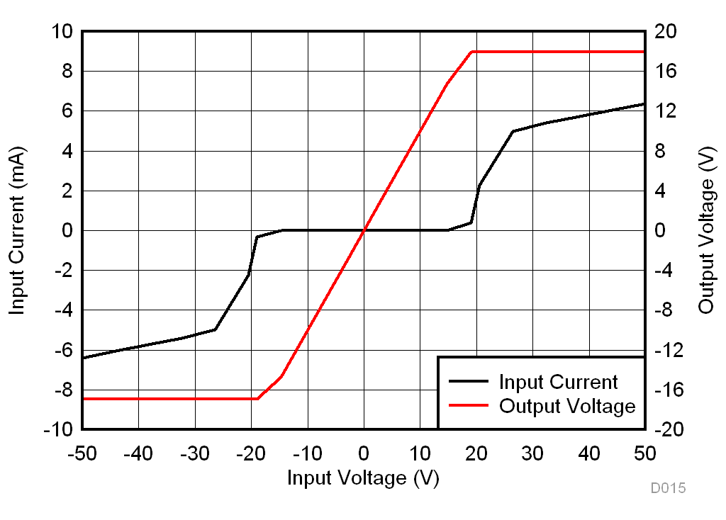
INA818 D015_SBOS959.gifFigure 63. Input Current vs Input Overvoltage