SLLS867K September 2007 – October 2015 ISO7230C , ISO7230M , ISO7231C , ISO7231M
PRODUCTION DATA.
- 1 Features
- 2 Applications
- 3 Description
- 4 Revision History
- 5 Device Comparison Table
- 6 Pin Configuration and Functions
-
7 Specifications
- 7.1 Absolute Maximum Ratings
- 7.2 ESD Ratings
- 7.3 Recommended Operating Conditions
- 7.4 Thermal Information
- 7.5 Electrical Characteristics: VCC1 and VCC2 at 5-V
- 7.6 Electrical Characteristics: VCC1 at 5-V, VCC2 at 3.3-V
- 7.7 Electrical Characteristics: VCC1 at 3.3-V, VCC2 at 5-V
- 7.8 Electrical Characteristics: VCC1 and VCC2 at 3.3 V
- 7.9 Power Dissipation Characteristics
- 7.10 Switching Characteristics: VCC1 and VCC2 at 5-V
- 7.11 Switching Characteristics: VCC1 at 5-V, VCC2 at 3.3-V
- 7.12 Switching Characteristics: VCC1 at 3.3-V and VCC2 at 5-V
- 7.13 Switching Characteristics: VCC1 and VCC2 at 3.3-V
- 7.14 Typical Characteristics
- 8 Parameter Measurement Information
- 9 Detailed Description
- 10Application and Implementation
- 11Power Supply Recommendations
- 12Layout
- 13Device and Documentation Support
- 14Mechanical, Packaging, and Orderable Information
パッケージ・オプション
デバイスごとのパッケージ図は、PDF版データシートをご参照ください。
メカニカル・データ(パッケージ|ピン)
- DW|16
サーマルパッド・メカニカル・データ
発注情報
9 Detailed Description
9.1 Overview
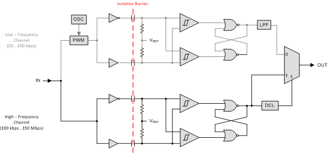
The isolator in Figure 13 is based on a capacitive isolation barrier technique. The I/O channel of the device consists of two internal data channels, a high-frequency channel (HF) with a bandwidth from 100 kbps up to 150 Mbps, and a low-frequency channel (LF) covering the range from 100 kbps down to DC. In principle, a single-ended input signal entering the HF-channel is split into a differential signal via the inverter gate at the input. The following capacitor-resistor networks differentiate the signal into transients, which then are converted into differential pulses by two comparators. The comparator outputs drive a NOR-gate flip-flop whose output feeds an output multiplexer. A decision logic (DCL) at the driving output of the flip-flop measures the durations between signal transients. If the duration between two consecutive transients exceeds a certain time limit, (as in the case of a low-frequency signal), the DCL forces the output-multiplexer to switch from the high- to the low-frequency channel.
Because low-frequency input signals require the internal capacitors to assume prohibitively large values, these signals are pulse-width modulated (PWM) with the carrier frequency of an internal oscillator, thus creating a sufficiently high frequency signal, capable of passing the capacitive barrier. As the input is modulated, a low-pass filter (LPF) is needed to remove the high-frequency carrier from the actual data before passing it on to the output multiplexer.
9.2 Functional Block Diagram
 Figure 13. Conceptual Block Diagram of a Digital Capacitive Isolator
9.3 Feature Description
9.3.1 Package Insulation and Safety-Related Specifications
| PARAMETER | TEST CONDITIONS | MIN | TYP | MAX | UNIT | |
|---|---|---|---|---|---|---|
| L(I01) | Minimum air gap (Clearance)(1) | Shortest terminal-to-terminal distance through air | 8 | mm | ||
| L(I02) | Minimum external tracking
(Creepage)(1) |
Shortest terminal-to-terminal distance across the package surface | 8 | mm | ||
| CTI | Tracking resistance (comparative tracking index) |
DIN EN 60112 (VDE 0303-11); IEC 60112 | 400 | V | ||
| DTI | Minimum Internal Gap (Internal Clearance) |
Distance through the insulation | 0.008 | mm | ||
| RIO(2) | Isolation resistance | Input to output, VIO = 500 V, TA = 25°C | >1012 | Ω | ||
| Input to output, VIO = 500 V, 100°C ≤ TA ≤ TA max | >1011 | Ω | ||||
| CIO(2) | Barrier capacitance Input to output | VI = 0.4 sin (4E6πt) | 2 | pF | ||
9.3.2 Insulation Characteristics
| PARAMETER | TEST CONDITIONS | SPECIFICATION | UNIT | |
|---|---|---|---|---|
| DIN V VDE V 0884-10 (VDE V 0884-10):2006-12(1) | ||||
| VIORM | Maximum repetitive peak isolation voltage | 560 | VPK | |
| VPR | Input to output test voltage | Method b1, VPR = VIORM x 1.875, 100% production test with t = 1 s, Partial discharge < 5 pC |
1050 | VPK |
| VIOTM | Maximum transient isolation voltage | VTEST = VIOTM, t = 60 s (qualification), t = 1 s (100% production) |
4000 | VPK |
| RS | Isolation resistance | VIO = 500 V at TS = 150 °C | >109 | Ω |
| Pollution degree | 2 | |||
| UL 1577 | ||||
| VISO | Withstanding isolation voltage | VTEST = VISO = 2500 VRMS, t = 60 s (qualification), VTEST = 1.2 x VISO = 3000 VRMS, t = 1 s (100% production) |
2500 | VRMS |
Table 1. IEC 60664-1 Ratings Table
| PARAMETER | TEST CONDITIONS | SPECIFICATION | ||
|---|---|---|---|---|
| Basic isolation group | Material group | II | ||
| Installation classification | Rated mains voltage ≤150 VRMS | I-IV | ||
| Rated mains voltage ≤300 VRMS | I-III | |||
9.3.3 Regulatory Information
9.3.4 Safety Limiting Values
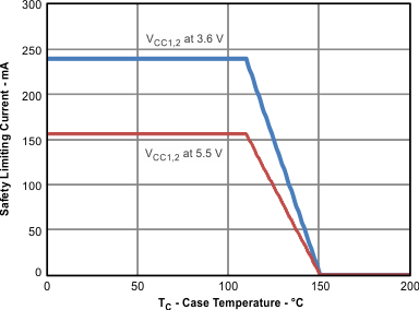
Safety limiting intends to prevent potential damage to the isolation barrier upon failure of input or output circuitry. A failure of the IO can allow low resistance to ground or the supply and, without current limiting, dissipate sufficient power to overheat the die and damage the isolation barrier potentially leading to secondary system failures.
| PARAMETER | TEST CONDITIONS | MIN | TYP | MAX | UNIT | ||
|---|---|---|---|---|---|---|---|
| IS | Safety input, output, or supply current | SOIC-16 | θJA = 168°C/W, VI = 5.5 V, TJ = 170°C, TA = 25°C | 156 | mA | ||
| θJA = 168°C/W, VI = 3.6 V, TJ = 170°C, TA = 25°C | 239 | ||||||
| TS | Maximum case temperature | SOIC-16 | 150 | °C | |||
The safety-limiting constraint is the absolute maximum junction temperature specified in the absolute maximum ratings table. The power dissipation and junction-to-air thermal impedance of the device installed in the application hardware determines the junction temperature. The assumed junction-to-air thermal resistance in the Thermal Characteristics table is that of a device installed in the JESD51-3, Low Effective Thermal Conductivity Test Board for Leaded Surface Mount Packages and is conservative. The power is the recommended maximum input voltage times the current. The junction temperature is then the ambient temperature plus the power times the junction-to-air thermal resistance.
 Figure 14. SOIC-16 ΘJC Thermal Derating Curve per VDE
9.4 Device Functional Modes
Table 2. Device Function Table ISO723x (1)
| VCCI | VCCO | INPUT (INx) |
OUTPUT ENABLE (ENx) |
OUTPUT (OUTx) |
|---|---|---|---|---|
| PU | PU | H | H or Open | H |
| L | H or Open | L | ||
| X | L | Z | ||
| Open | H or Open | H | ||
| PD | PU | X | H or Open | H |
| PD | PU | X | L | Z |
| X | PD | X | X | Undetermined |
