SLLS867K September 2007 – October 2015 ISO7230C , ISO7230M , ISO7231C , ISO7231M
PRODUCTION DATA.
- 1 Features
- 2 Applications
- 3 Description
- 4 Revision History
- 5 Device Comparison Table
- 6 Pin Configuration and Functions
-
7 Specifications
- 7.1 Absolute Maximum Ratings
- 7.2 ESD Ratings
- 7.3 Recommended Operating Conditions
- 7.4 Thermal Information
- 7.5 Electrical Characteristics: VCC1 and VCC2 at 5-V
- 7.6 Electrical Characteristics: VCC1 at 5-V, VCC2 at 3.3-V
- 7.7 Electrical Characteristics: VCC1 at 3.3-V, VCC2 at 5-V
- 7.8 Electrical Characteristics: VCC1 and VCC2 at 3.3 V
- 7.9 Power Dissipation Characteristics
- 7.10 Switching Characteristics: VCC1 and VCC2 at 5-V
- 7.11 Switching Characteristics: VCC1 at 5-V, VCC2 at 3.3-V
- 7.12 Switching Characteristics: VCC1 at 3.3-V and VCC2 at 5-V
- 7.13 Switching Characteristics: VCC1 and VCC2 at 3.3-V
- 7.14 Typical Characteristics
- 8 Parameter Measurement Information
- 9 Detailed Description
- 10Application and Implementation
- 11Power Supply Recommendations
- 12Layout
- 13Device and Documentation Support
- 14Mechanical, Packaging, and Orderable Information
パッケージ・オプション
デバイスごとのパッケージ図は、PDF版データシートをご参照ください。
メカニカル・データ(パッケージ|ピン)
- DW|16
サーマルパッド・メカニカル・データ
発注情報
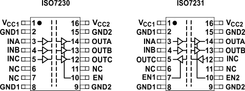
6 Pin Configuration and Functions
DW Package
16-Pin SOIC
Top View

Pin Functions
| PIN | TYPE | DESCRIPTION | ||
|---|---|---|---|---|
| NAME | ISO7230 | ISO7231 | ||
| EN | 10 | – | I | Enable, channel A, B, and C |
| EN1 | – | 7 | I | Enable, channel C |
| EN2 | – | 10 | I | Enable, channel A and B |
| GND1 | 2, 8 | 2, 8 | – | Ground connection for VCC1 |
| GND2 | 9, 15 | 9. 15 | – | Ground connection for VCC2 |
| INA | 3 | 3 | I | Input, channel A |
| INB | 4 | 4 | I | Input, channel B |
| INC | 5 | 12 | I | Input, channel C |
| NC | 6, 7, 11 | 6, 11 | – | Not connected |
| OUTA | 14 | 14 | O | Output, channel A |
| OUTB | 13 | 13 | O | Output, channel B |
| OUTC | 12 | 5 | O | Output, channel C |
| VCC1 | 1 | 1 | – | Power supply, VCC1 |
| VCC2 | 16 | 16 | – | Power supply, VCC2 |