SNVS033D May 2004 – November 2015 LM2621
PRODUCTION DATA.
- 1 Features
- 2 Applications
- 3 Description
- 4 Revision History
- 5 Pin Configuration and Functions
- 6 Specifications
- 7 Detailed Description
-
8 Application and Implementation
- 8.1 Application Information
- 8.2 Typical Applications
- 9 Power Supply Recommendations
- 10Layout
- 11Device and Documentation Support
- 12Mechanical, Packaging, and Orderable Information
6 Specifications
6.1 Absolute Maximum Ratings
See (1)(3)| MIN | MAX | UNIT | |
|---|---|---|---|
| SW Pin Voltage | –0.5 | 14.5 | V |
| BOOT, VDD, EN and FB Pins | –0.5 | 10 | V |
| FREQ Pin | 100 | µA | |
| Power Dissipation (TA=25°C) (2) | 500 | mW | |
| TJmax(2) | 150 | °C | |
| Lead Temp. (Soldering, 5 sec) | 260 | °C | |
| Storage temperature, Tstg | –65 | 150 | °C |
(1) Stresses beyond those listed under Absolute Maximum Ratings may cause permanent damage to the device. These are stress ratings only, which do not imply functional operation of the device at these or any other conditions beyond those indicated under Recommended Operating Conditions. Exposure to absolute-maximum-rated conditions for extended periods may affect device reliability.
(2) The maximum power dissipation must be derated at elevated temperatures and is dictated by Tjmax (maximum junction temperature), θJA (junction to ambient thermal resistance), and TA (ambient temperature). The maximum allowable power dissipation at any temperature is Pdmax = (Tjmax - TA)/ θJA or the number given in the Absolute Maximum Ratings, whichever is lower.
(3) If Military/Aerospace specified devices are required, please contact the Texas Instruments Sales Office/ Distributors for availability and specifications.
6.2 Recommended Operating Conditions
over operating free-air temperature range (unless otherwise noted)| MIN | NOM | MAX | UNIT | |
|---|---|---|---|---|
| VDD | 2.5 | 5 | V | |
| FB | 0 | VDD | V | |
| EN | 0 | VDD | V | |
| BOOT | 0 | 10 | V | |
| Ambient Temperature, TA | –40 | 85 | °C |
6.3 Thermal Information
| THERMAL METRIC(1) | LM2621 | UNIT | |
|---|---|---|---|
| DGK (VSSOP) | |||
| 8 PINS | |||
| RθJA | Junction-to-ambient thermal resistance (2) | 160 | °C/W |
| RθJC(top) | Junction-to-case (top) thermal resistance | 52.7 | °C/W |
| RθJB | Junction-to-board thermal resistance | 80.1 | °C/W |
| ψJT | Junction-to-top characterization parameter | 5.5 | °C/W |
| ψJB | Junction-to-board characterization parameter | 78.8 | °C/W |
| RθJC(bot) | Junction-to-case (bottom) thermal resistance | N/A | °C/W |
(1) For more information about traditional and new thermal metrics, see the Semiconductor and IC Package Thermal Metrics application report, SPRA953.
6.4 Electrical Characteristics
Unless otherwise specified: VDD= VOUT= 3.3 V, TJ = 25°C.| PARAMETER | TEST CONDITIONS | MIN | TYP | MAX | UNIT | |
|---|---|---|---|---|---|---|
| VIN_ST | Minimum Start-Up Supply Voltage(1) | ILOAD = 0 mA | 1.1 | V | ||
| ILOAD = 0 mA, –40°C to 85°C | 1.2 | |||||
| VIN_OP | Minimum Operating Supply Voltage (once started) | ILOAD = 0 mA | 0.65 | V | ||
| VFB | FB Pin Voltage | 1.24 | V | |||
| –40°C to 85°C | 1.2028 | 1.2772 | ||||
| VOUT_MAX | Maximum Output Voltage | 14 | V | |||
| VHYST | Hysteresis Voltage(2) | 30 | mV | |||
| –40°C to 85°C | 45 | |||||
| η | Efficiency | VIN = 3.6 V; VOUT = 5 V; ILOAD = 500 mA | 87% | |||
| VIN = 2.5 V; VOUT = 3.3 V; ILOAD = 200 mA | 87% | |||||
| D | Switch Duty Cycle | 70% | ||||
| −40°C to 85°C | 60% | 80% | ||||
| IDD | Operating Quiescent Current(3) | FB Pin > 1.3 V; EN Pin at VDD | 80 | µA | ||
| FB Pin > 1.3 V; EN Pin at VDD, –40°C to 85°C | 110 | |||||
| ISD | Shutdown Quiescent Current(4) | VDD, BOOT and SW Pins at 5.0 V; EN Pin < 200 mV | 0.01 | µA | ||
| VDD, BOOT and SW Pins at 5.0 V; EN Pin < 200 mV, –40°C to 85°C | 2.5 | |||||
| ICL | Switch Peak Current Limit | 2.85 | A | |||
| RDS_ON | MOSFET Switch On Resistance | 0.17 | Ω | |||
| ENABLE SECTION | ||||||
| VEN_LO | EN Pin Voltage Low(5) | –40°C to 85°C | 0.15VDD | V | ||
| VEN_HI | EN Pin Voltage High(5) | –40°C to 85°C | 0.7VDD | V | ||
(1) Output in regulation, VOUT = VOUT (NOMINAL) ± 5%
(2) This is the hysteresis value of the internal comparator used for the gated-oscillator control scheme.
(3) This is the current into the VDD pin.
(4) This is the total current into pins VDD, BOOT, SW and FREQ.
(5) When the EN pin is below VEN_LO, the regulator is shut down; when it is above VEN_HI, the regulator is operating.
6.5 Typical Characteristics
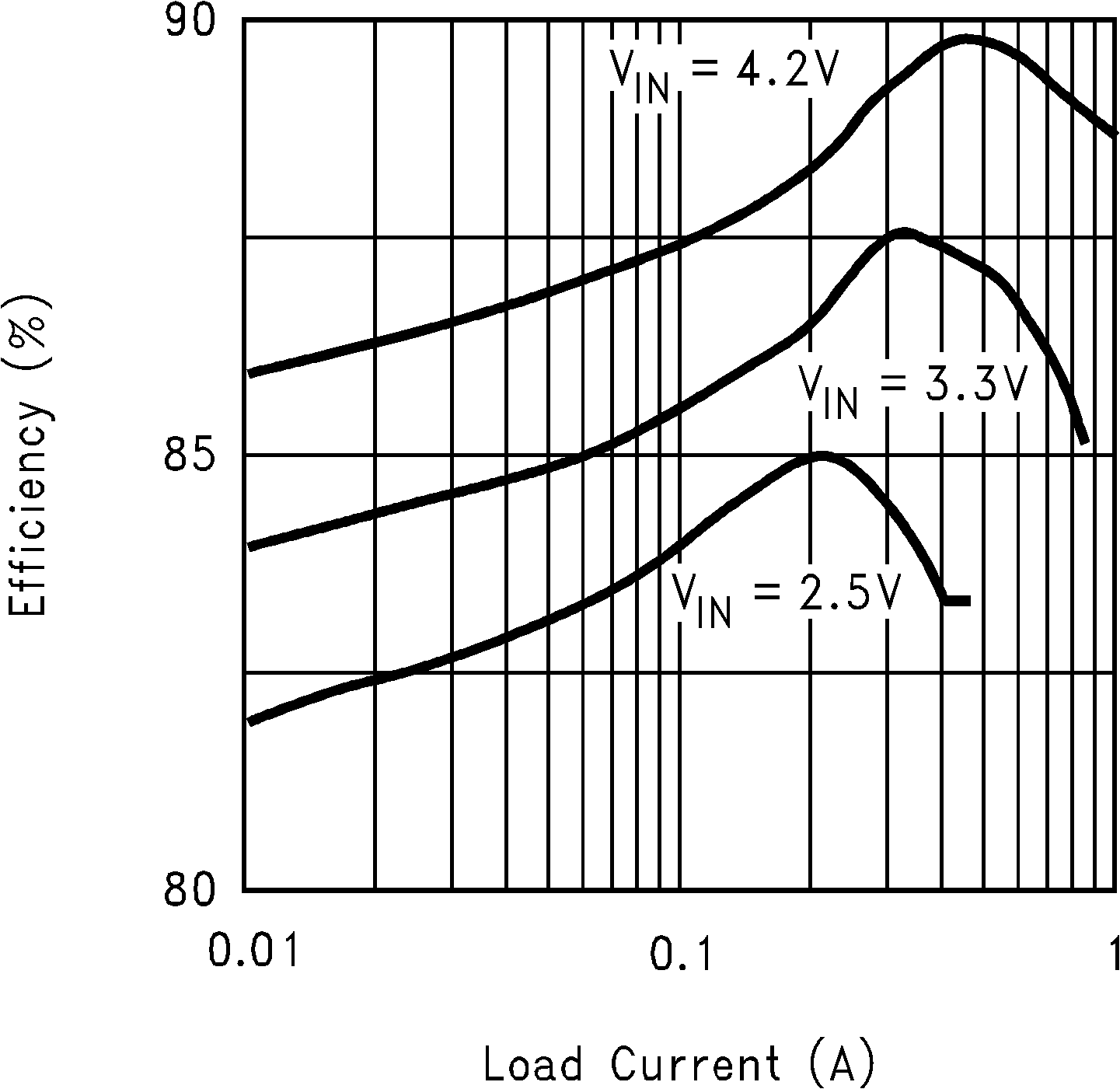
| VOUT = 5.0 V |
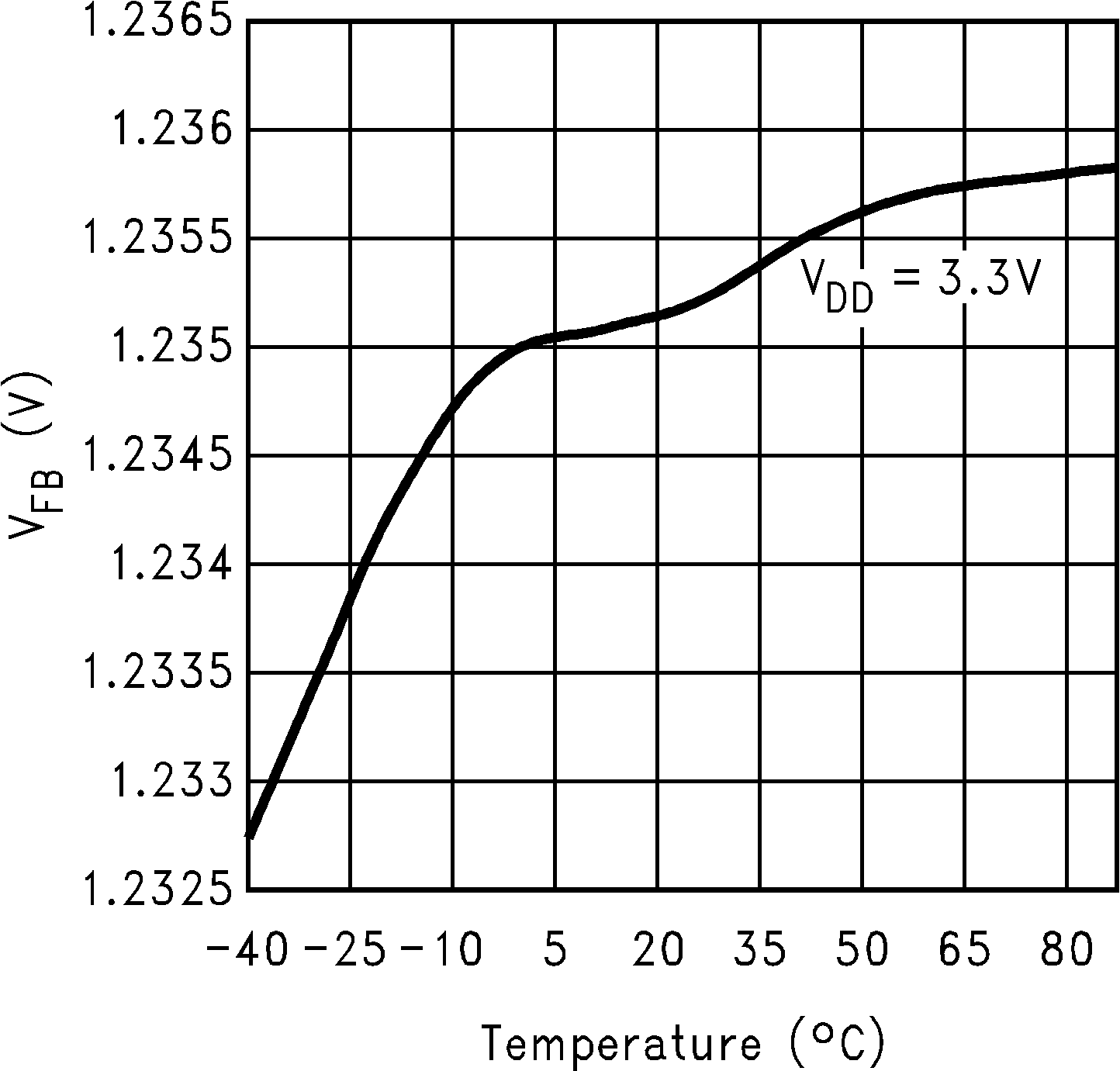 Figure 3. VFB vs Temperature
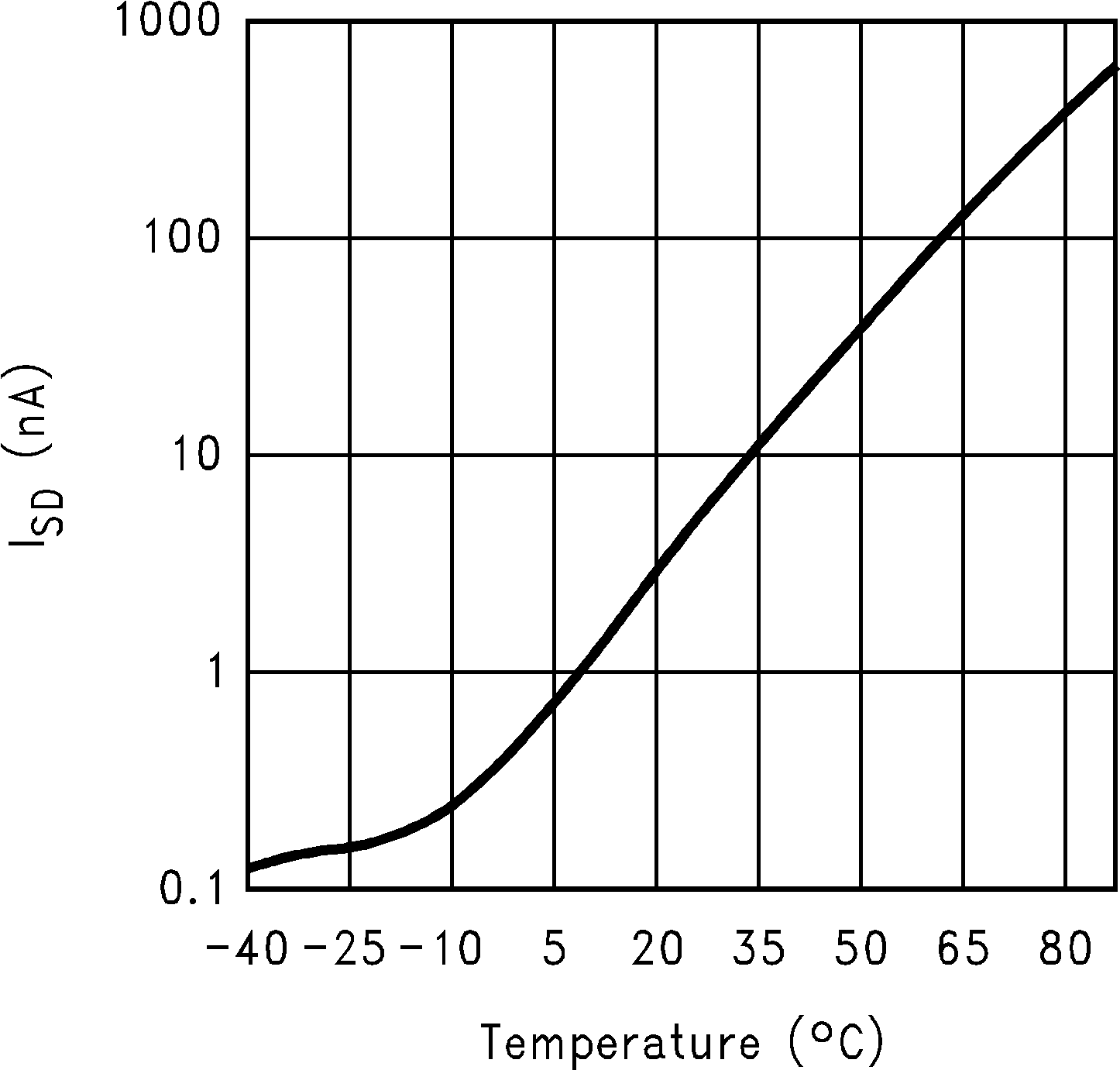 Figure 5. ISD vs Temperature
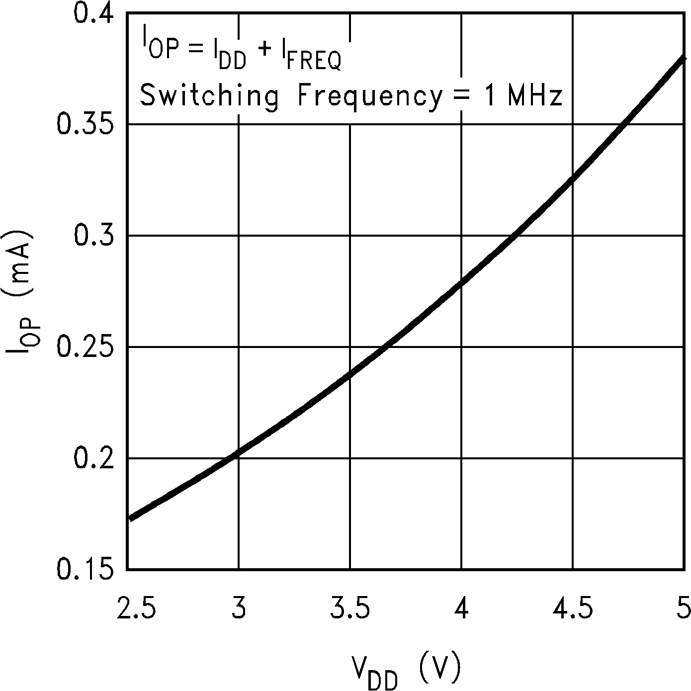
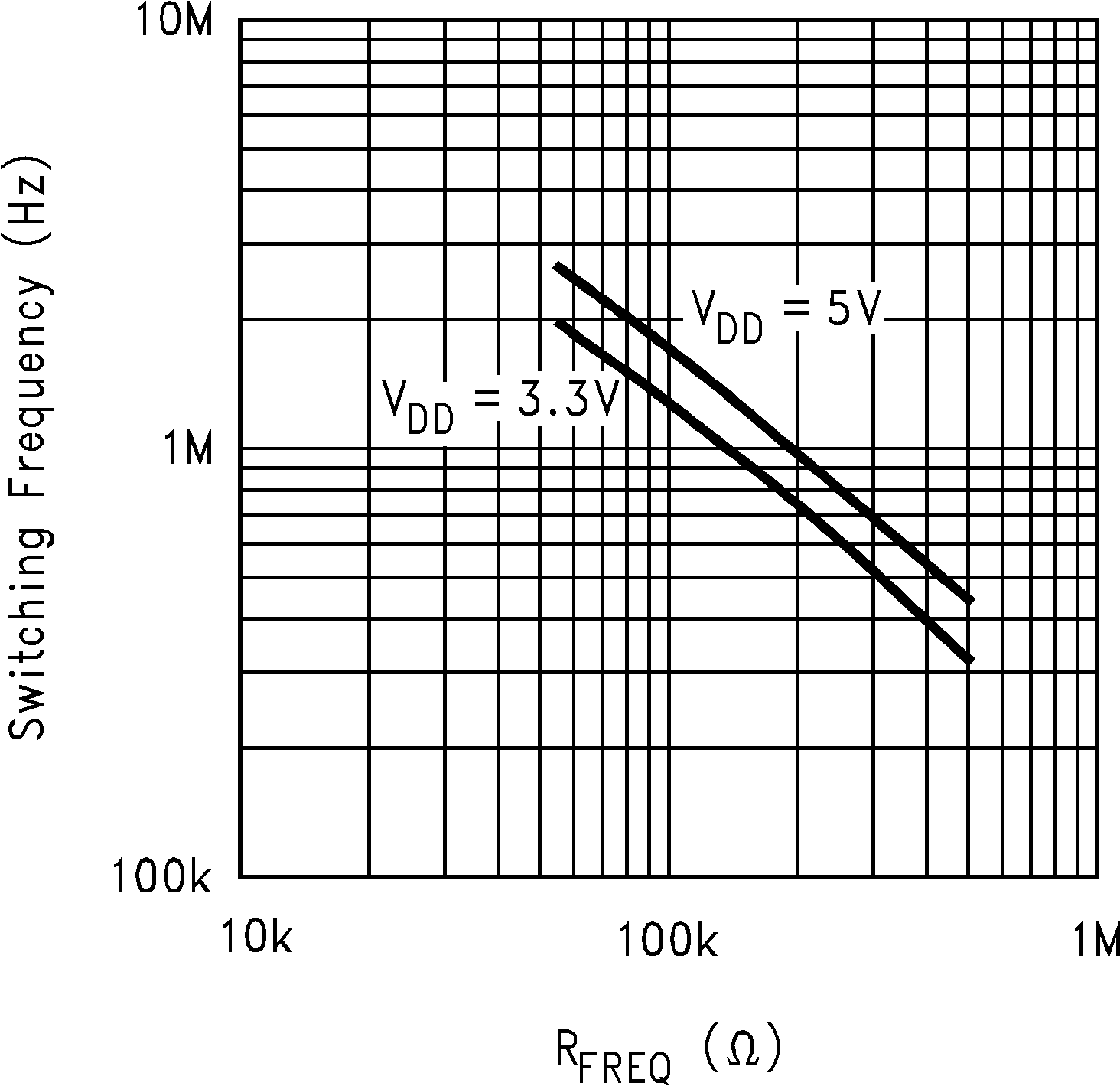 Figure 9. Switching Frequency vs RFQ
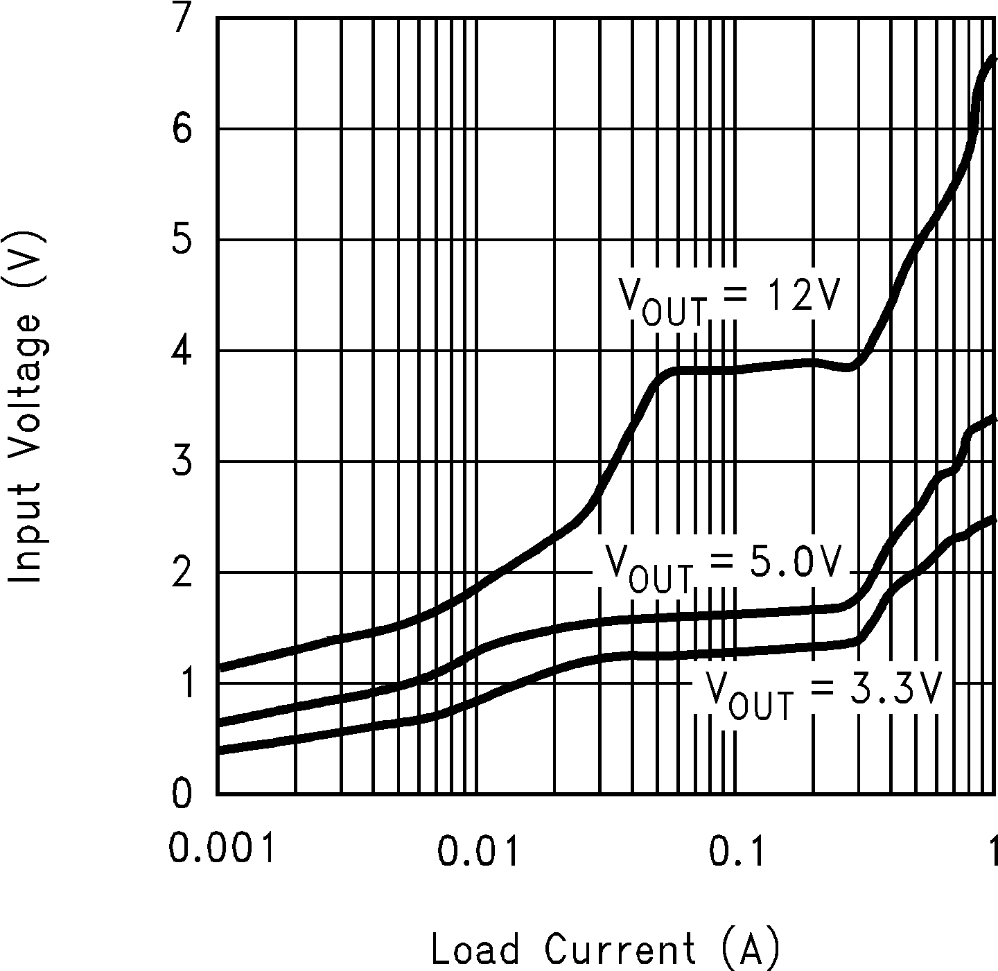 Figure 11. Maximum Load Current vs Input Voltage
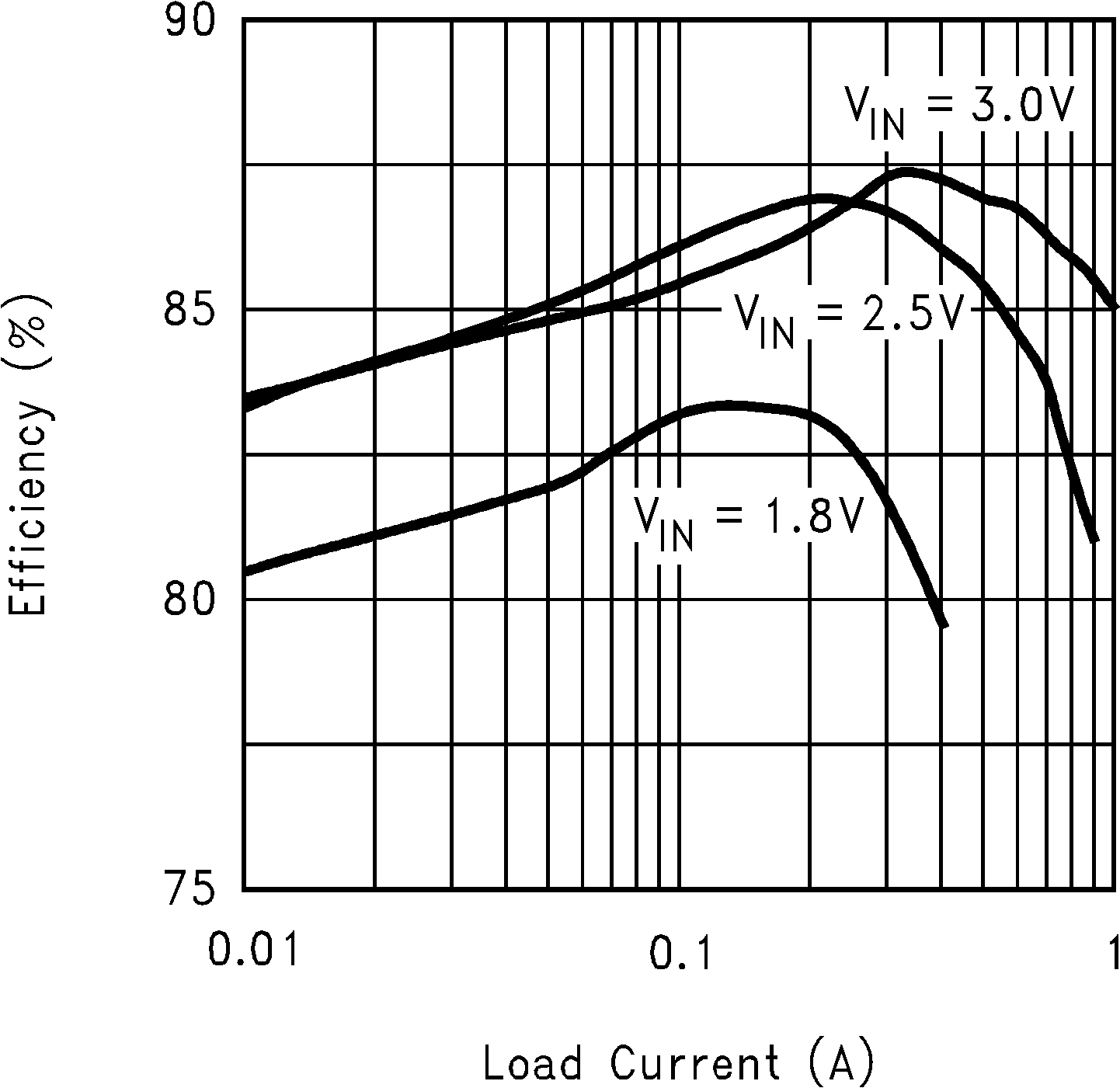
| VOUT = 3.3 V |
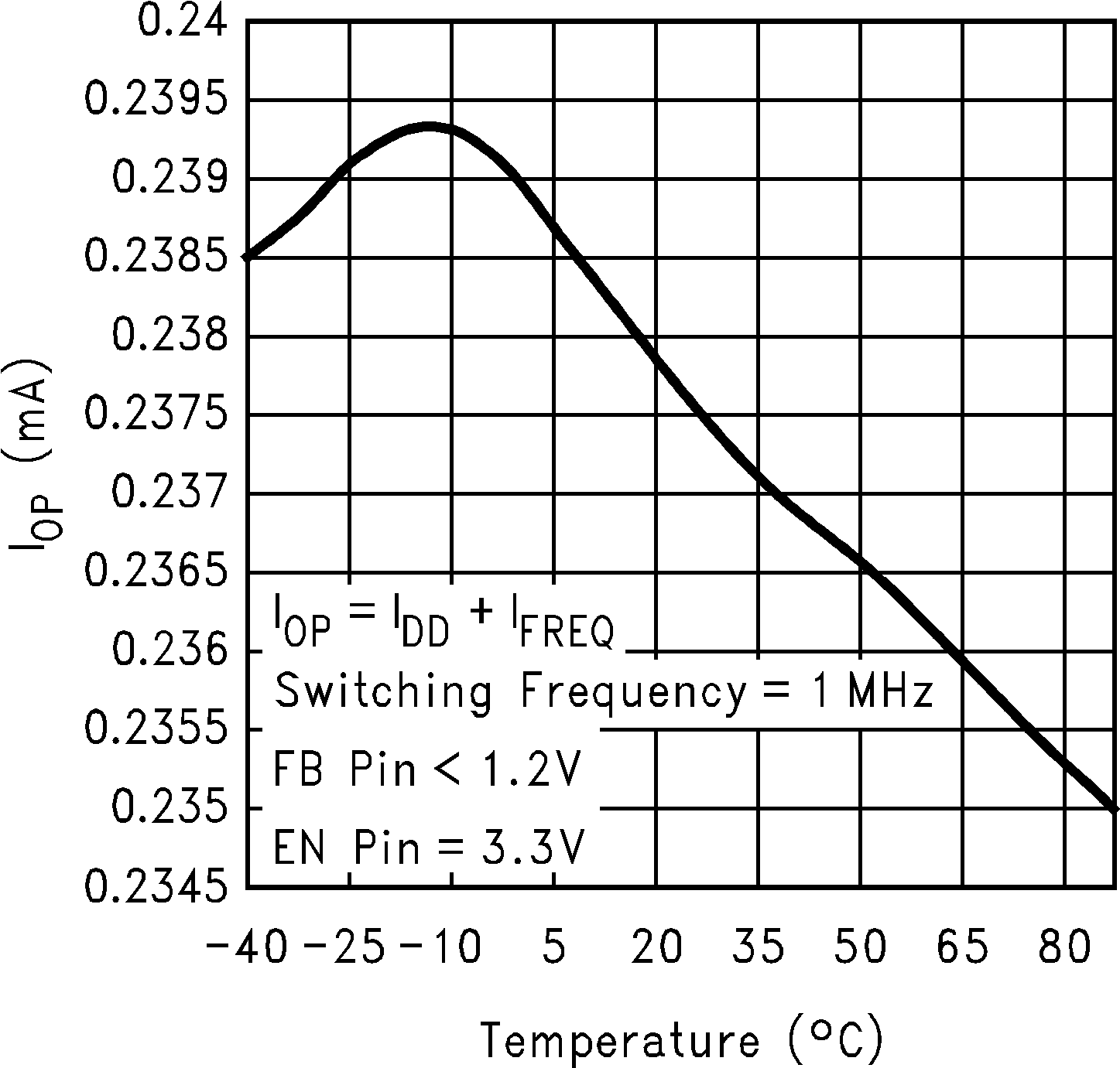 Figure 4. IOP vs Temperature
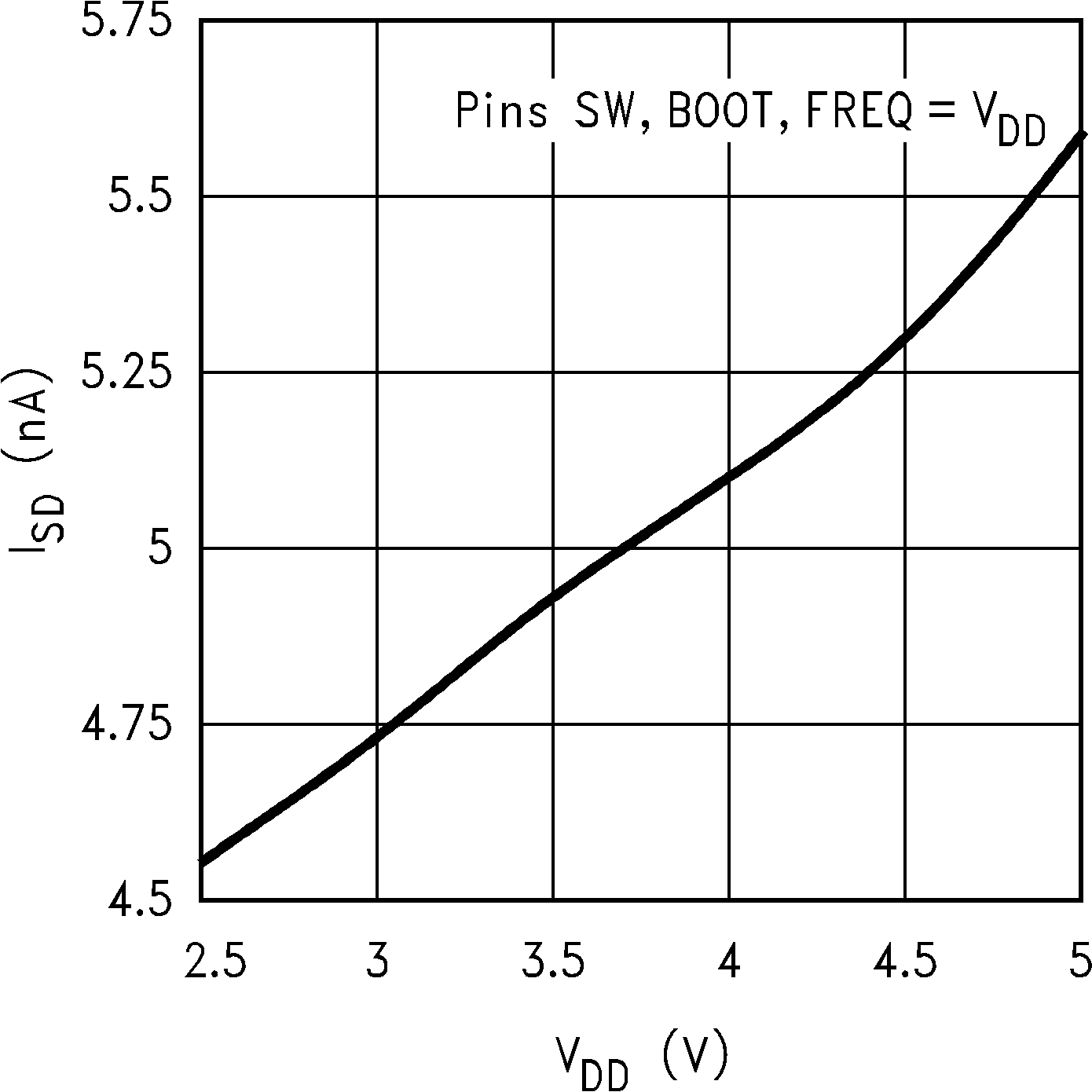 Figure 6. ISD vs VDD
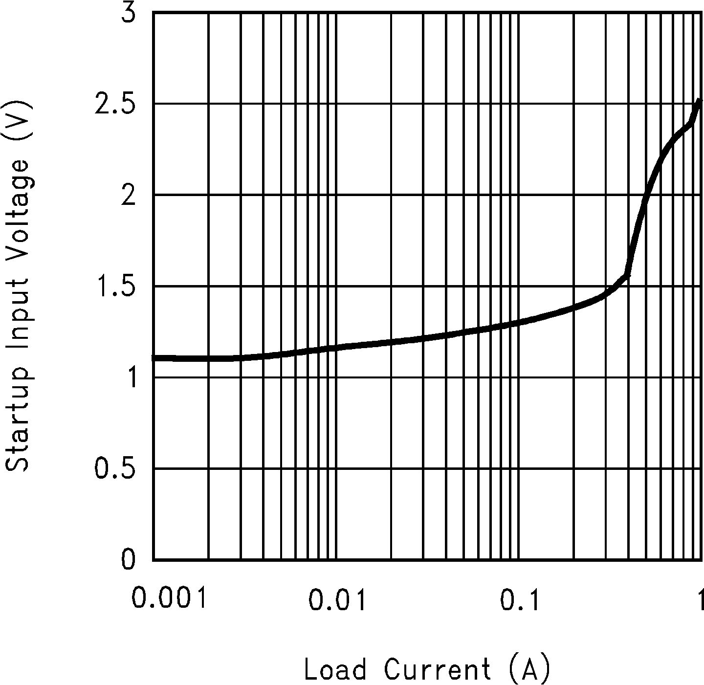
| VOUT = 3.3 V |
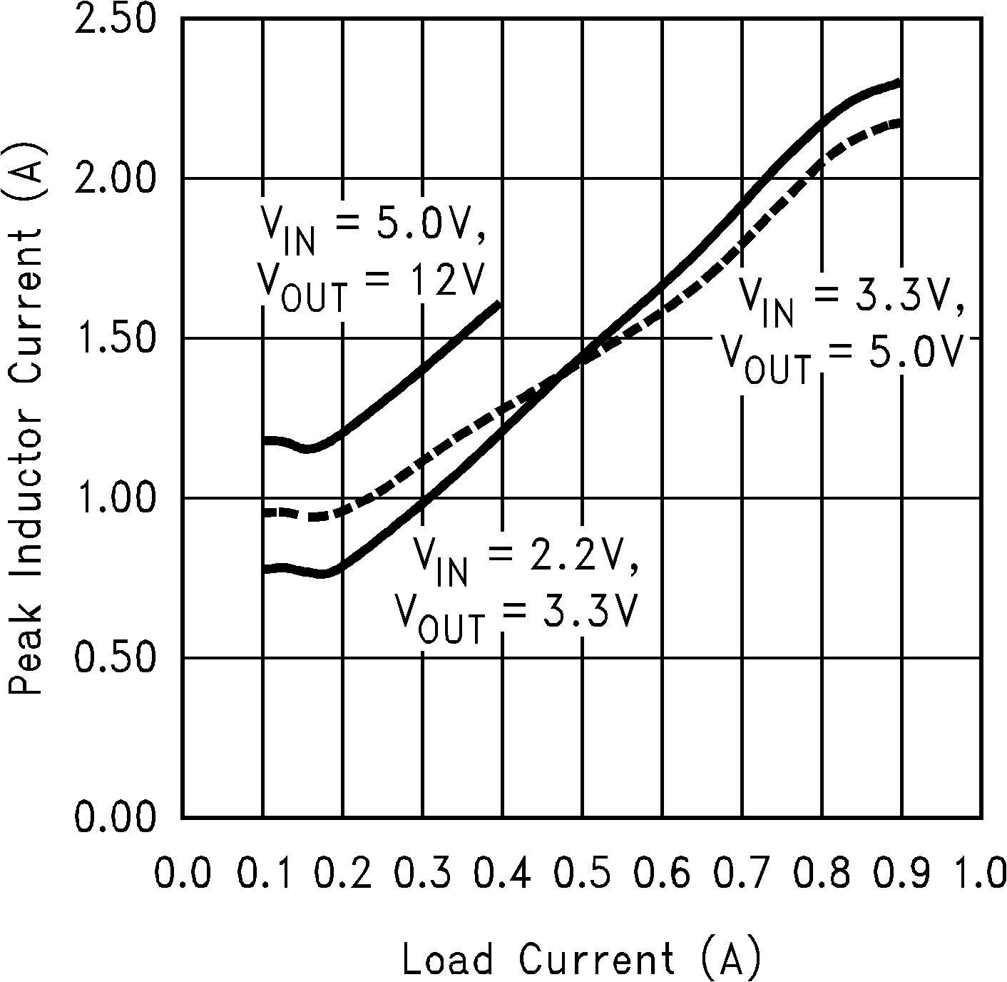 Figure 10. Peak Inductor Current vs Load Current