SNVS135E September 1999 – December 2014 LM2660
PRODUCTION DATA.
- 1 Features
- 2 Applications
- 3 Description
- 4 Revision History
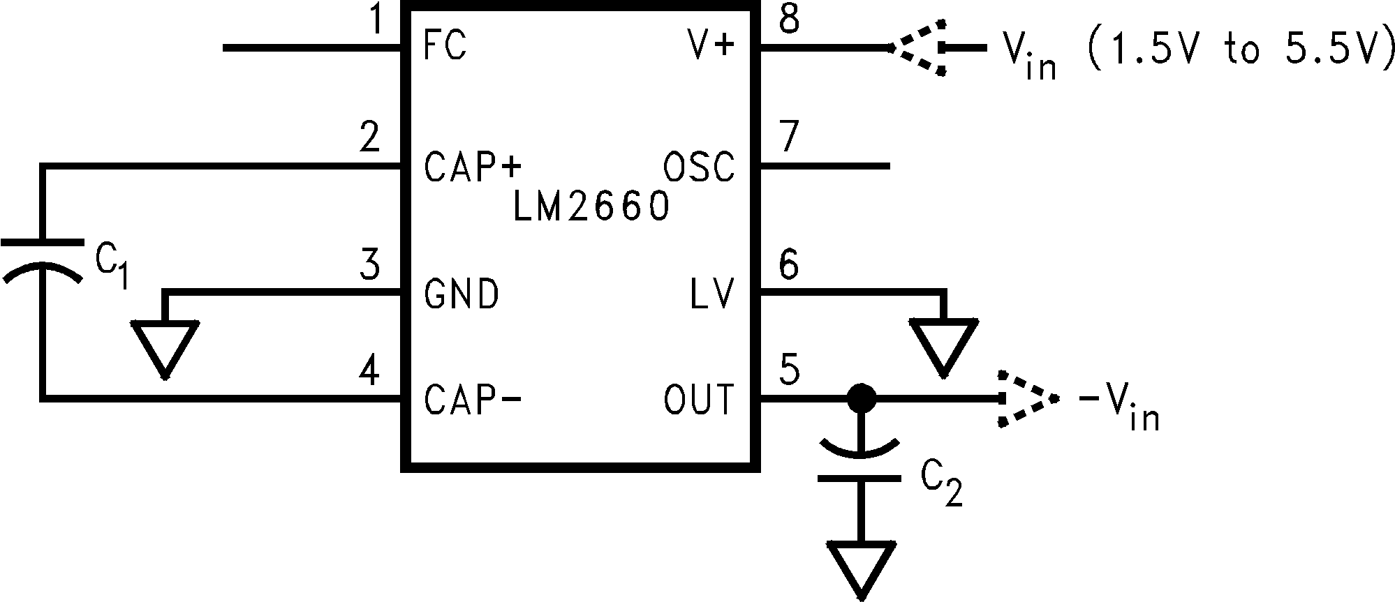
- 5 Pin Configuration and Functions
- 6 Specifications
- 7 Parameter Measurement Information
- 8 Detailed Description
- 9 Application and Implementation
- 10Power Supply Recommendations
- 11Layout
- 12Device and Documentation Support
- 13Mechanical, Packaging, and Orderable Information
パッケージ・オプション
メカニカル・データ(パッケージ|ピン)
サーマルパッド・メカニカル・データ
- DGK|8
発注情報
1 Features
- Inverts or Doubles Input Supply Voltage
- Narrow SOIC and VSSOP Packages
- 6.5-Ω Typical Output Resistance
- 88% Typical Conversion Efficiency at 100 mA
- Selectable Oscillator Frequency: 10 kHz/80 kHz
- Optional External Oscillator Input
2 Applications
- Laptop Computers
- Cellular Phones
- Medical Instruments
- Operational Amplifier Power Supplies
- Interface Power Supplies
- Handheld Instruments
3 Description
The LM2660 CMOS charge-pump voltage converter is a versatile unregulated switched capacitor inverter or doubler. Operating from a wide 1.5-V to 5.5-V supply voltage, the LM2660 uses two low-cost capacitors to provide 100 mA of output current without the cost, size and EMI related to inductor-based converters. With an operating current of only 120 µA and operating efficiency greater than 90% at most loads, the LM2660 provides ideal performance for battery-powered systems. LM2660 devices can be operated directly in parallel to lower output impedance, thus providing more current at a given voltage.
The FC (frequency control) pin selects between a nominal 10-kHz or 80-kHz oscillator frequency. The oscillator frequency can be lowered by adding an external capacitor to the OSC pin. Also, the OSC pin may be used to drive the LM2660 with an external clock up to 150 kHz. Through these methods, output ripple frequency and harmonics may be controlled.
Additionally, the LM2660 may be configured to divide a positive input voltage precisely in half. In this mode, input voltages as high as 11 V may be used.
Device Information(1)
| PART NUMBER | PACKAGE | BODY SIZE (NOM) |
|---|---|---|
| LM2660 | SOIC (8) | 4.90 mm x 3.91 mm |
| VSSOP (8) | 3.00 mm x 3.00 mm |
- For all available packages, see the orderable addendum at the end of the datasheet.
Simplified Schematic
4 Revision History
Changes from D Revision (May 2013) to E Revision
- Added Device Information and Handling Rating tables, Feature Description, Device Functional Modes, Application and Implementation, Power Supply Recommendations, Layout, Device and Documentation Support, and Mechanical, Packaging, and Orderable Information sections; moved some curves to Application Curves section Go
Changes from C Revision (May 2013) to D Revision
- Changed layout of National Data Sheet to TI formatGo