SNVS135E September 1999 – December 2014 LM2660
PRODUCTION DATA.
- 1 Features
- 2 Applications
- 3 Description
- 4 Revision History
- 5 Pin Configuration and Functions
- 6 Specifications
- 7 Parameter Measurement Information
- 8 Detailed Description
- 9 Application and Implementation
- 10Power Supply Recommendations
- 11Layout
- 12Device and Documentation Support
- 13Mechanical, Packaging, and Orderable Information
パッケージ・オプション
メカニカル・データ(パッケージ|ピン)
サーマルパッド・メカニカル・データ
- DGK|8
発注情報
11 Layout
11.1 Layout Guidelines
The high switching frequency and large switching currents of the LM2660 make the choice of layout important. The following steps should be used as a reference to ensure the device is stable and maintains proper LED current regulation across its intended operating voltage and current range:
- Place CIN on the top layer (same layer as the LM2660) and as close to the device as possible. Connecting the input capacitor through short, wide traces to both the V+ and GND pins reduces the inductive voltage spikes that occur during switching which can corrupt the V+ line.
- Place COUT on the top layer (same layer as the LM2660) and as close as possible to the OUT and GND pin. The returns for both CIN and COUT should come together at one point, as close to the GND pin as possible. Connecting COUT through short, wide traces reduce the series inductance on the OUT and GND pins that can corrupt the VOUT and GND lines and cause excessive noise in the device and surrounding circuitry.
- Place C1 on the top layer (same layer as the LM2660) and as close to the device as possible. Connect the flying capacitor through short, wide traces to both the CAP+ and CAP– pins.
11.2 Layout Example
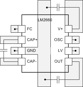 Figure 25. LM2660 Layout Example