SNVS005E November 1999 – December 2014 LM2664
PRODUCTION DATA.
- 1 Features
- 2 Applications
- 3 Description
- 4 Revision History
- 5 Pin Configuration and Functions
- 6 Specifications
- 7 Parameter Measurement Information
- 8 Detailed Description
- 9 Application and Implementation
- 10Power Supply Recommendations
- 11Layout
- 12Device and Documentation Support
- 13Mechanical, Packaging, and Orderable Information
8 Detailed Description
8.1 Overview
The LM2664 CMOS charge-pump voltage converter inverts a positive voltage in the range of 1.8 V to 5.5 V to the corresponding negative voltage of −1.8 V to −5.5 V. The LM2664 uses two low-cost capacitors to provide up to 40 mA of output current.
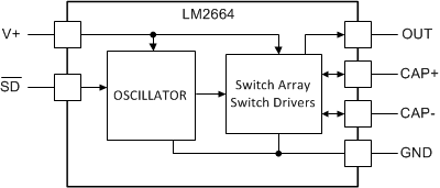
8.2 Functional Block Diagram
8.3 Feature Description
The LM2664 contains four large CMOS switches which are switched in a sequence to invert the input supply voltage. Energy transfer and storage are provided by external capacitors. Figure 10 illustrates the voltage conversion scheme. When S1 and S3 are closed, C1 charges to the supply voltage V+. During this time interval, switches S2 and S4 are open. In the second time interval, S1 and S3 are open; at the same time, S2 and S4 are closed, C1 is charging C2. After a number of cycles, the voltage across C2 will be pumped to V+. Since the anode of C2 is connected to ground, the output at the cathode of C2 equals −(V+) when there is no load current. The output voltage drop when a load is added is determined by the parasitic resistance (Rds(on) of the MOSFET switches and the ESR of the capacitors) and the charge transfer loss between capacitors. Details will be discussed in the following application information section.
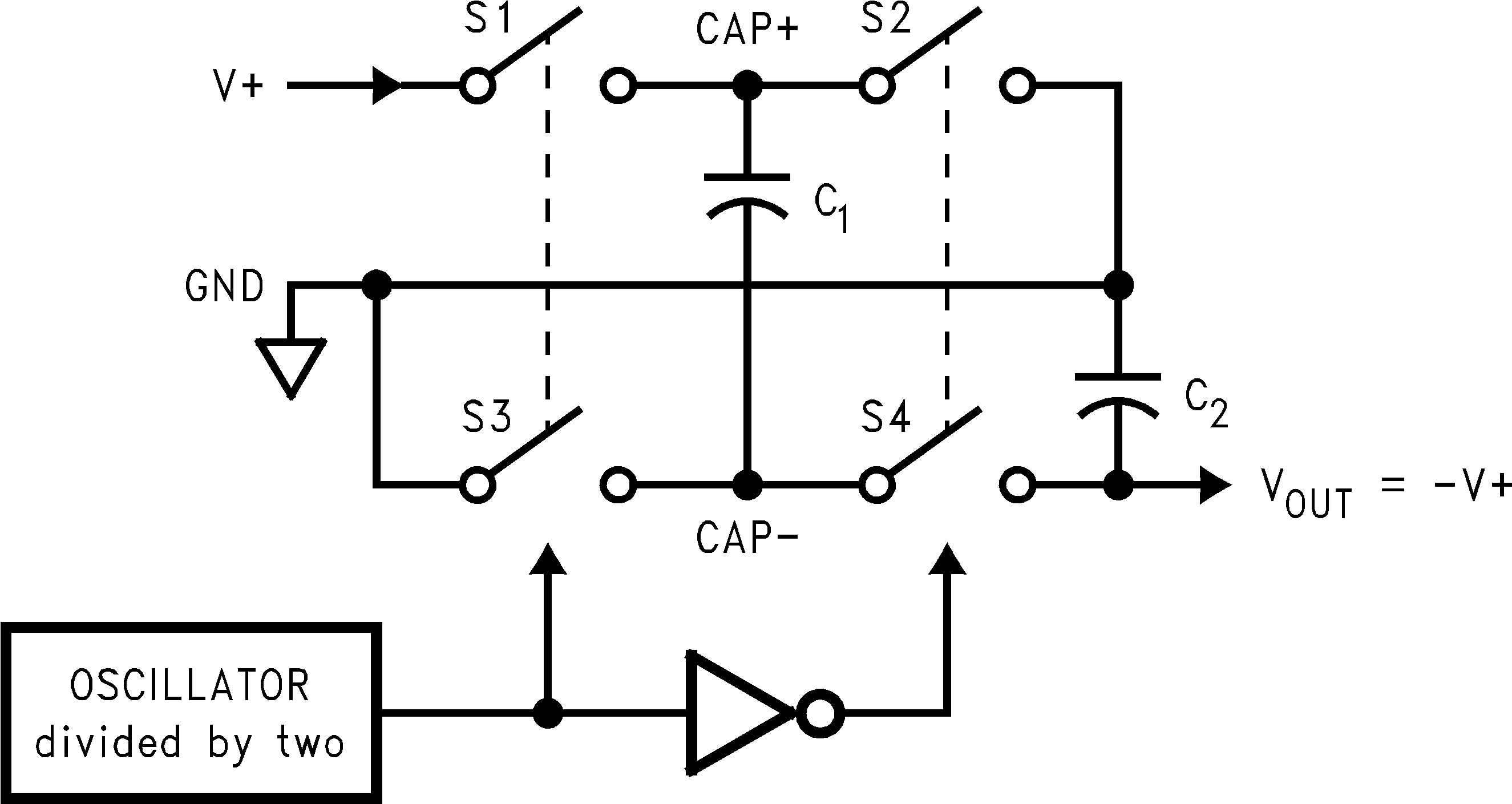 Figure 10. Voltage Inverting Principle
8.4 Device Functional Modes
8.4.1 Shutdown Mode
A shutdown (SD) pin is available to disable the device and reduce the quiescent current to 1 µA. Applying a voltage less than 20% of V+ to the SD pin will bring the device into shutdown mode. While in normal operating mode, the pin is connected to V+.