SNVS896B August 2013 – November 2014 LM27403
PRODUCTION DATA.
- 1 Features
- 2 Applications
- 3 Description
- 4 Revision History
- 5 Description (Continued)
- 6 Pin Configuration and Functions
- 7 Specifications
-
8 Detailed Description
- 8.1 Overview
- 8.2 Functional Block Diagram
- 8.3
Feature Description
- 8.3.1 Input Range: VIN
- 8.3.2 Output Voltage: FB Voltage and Accuracy
- 8.3.3 Input and Bias Rail Voltages: VIN and VDD
- 8.3.4 Precision Enable: UVLO/EN
- 8.3.5 Switching Frequency
- 8.3.6 Temperature Sensing: D+ and D-
- 8.3.7 Thermal Shutdown: OTP
- 8.3.8 Inductor-DCR-Based Overcurrent Protection
- 8.3.9 Current Sensing: CS+ and CS-
- 8.3.10 Current Limit Handling
- 8.3.11 Soft-Start: SS/TRACK
- 8.3.12 Monotonic Startup
- 8.3.13 Prebias Startup
- 8.3.14 Voltage-Mode Control
- 8.3.15 Output Voltage Remote Sense: RS
- 8.3.16 Power Good: PGOOD
- 8.3.17 Gate Drivers: LG and HG
- 8.3.18 Sink and Source Capability
- 8.4 Device Functional Modes
-
9 Application and Implementation
- 9.1 Application Information
- 9.2
Typical Applications
- 9.2.1 Design 1 - High-Efficiency Synchronous Buck Regulator for Telecom Power
- 9.2.2 Design 2 - Powering FPGAs Using Flexible 30A Regulator With Small Footprint
- 9.2.3 Design 3 - Powering Multicore DSPs
- 9.2.4 Design 4 - Regulated 12-V Rail with LDO Low-Noise Auxiliary Output for RF Power
- 9.2.5 Design 5 - High Power Density Implementation From 3.3-V or 5-V Supply Rail
- 10Power Supply Recommendations
- 11Layout
- 12Device and Documentation Support
- 13Mechanical, Packaging, and Orderable Information
パッケージ・オプション
メカニカル・データ(パッケージ|ピン)
- RTW|24
サーマルパッド・メカニカル・データ
- RTW|24
発注情報
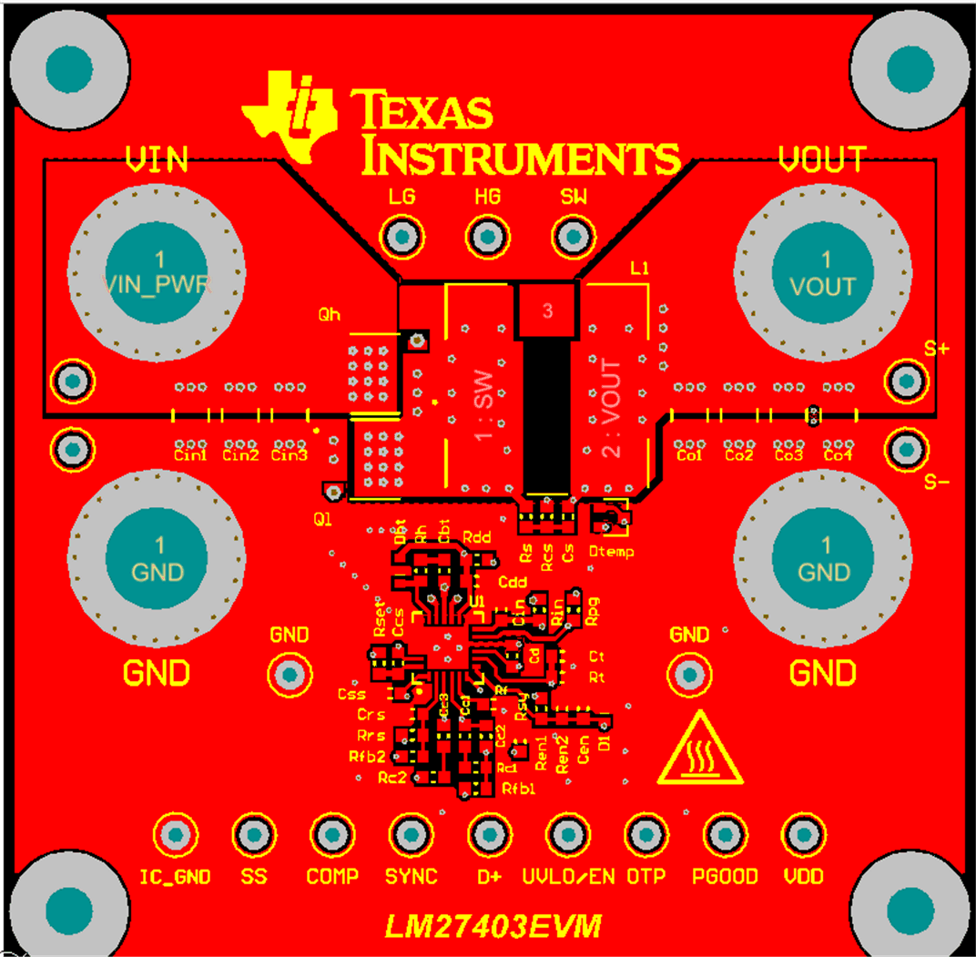
11 Layout
11.1 Layout Guidelines
Proper PCB design and layout is important in a high current, fast switching circuit (with high current and voltage slew rates) to assure appropriate device operation and design robustness. As expected, certain issues must be considered before designing a PCB layout using the LM27403. The main switching loop of the power stage is denoted by #1 in Figure 51. The topological architecture of a buck converter means that particularly high di/dt current will flow in loop #1, and it becomes mandatory to reduce the parasitic inductance of this loop by minimizing its effective loop area. For loop #2 however, the di/dt through inductor L1 and capacitor COUT is naturally limited by the inductor. Keeping the area of loop #2 small is not nearly as important as that of loop #1. Also important are the gate drive loops of the low-side and high-side MOSFETs, denoted by #3 and #4, respectively, in Figure 51.
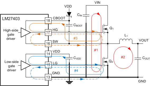 Figure 51. DC-DC Regulator Ground System With Power Stage and Gate Drive Circuit Switching Loops
11.1.1 Power Stage Layout
- Input capacitor(s), output capacitor(s) and MOSFETs are the constituent components in the power stage of a buck regulator and are typically placed on the top side of the PCB (solder side). Leveraging any system-level airflow, the benefits of convective heat transfer are thus maximized. In a two-sided PCB layout, small-signal components are typically placed on the bottom side (component side). At least one inner plane should be inserted, connected to ground, in order to shield and isolate the small-signal traces from noisy power traces and lines.
- The DC-DC converter has several high-current loops. Minimize the area of these loops in order to suppress generated switching noise and parasitic loop inductance and optimize switching performance.
- Loop #1: The most important loop to minimize the area of is the path from the input capacitor(s) through the high- and low-side MOSFETs, and back to the capacitor(s) through the ground connection. Connect the input capacitor(s) negative terminal close to the source of the low-side MOSFET (at ground). Similarly, connect the input capacitor(s) positive terminal close to the drain of the high-side MOSFET (at VIN). Refer to loop #1 of Figure 51.
- Loop #2. The second important loop is the path from the low-side MOSFET through inductor and output capacitor(s), and back to source of the low-side MOSFET through ground. Connect source of the low-side MOSFET and negative terminal of the output capacitor(s) at ground as close as possible. Refer to loop #2 of Figure 51.
- The PCB trace defined as SW node, which connects to the source of the high-side (control) MOSFET, the drain of the low-side (synchronous) MOSFET and the high-voltage side of the inductor, should be short and wide. However, the SW connection is a source of injected EMI and thus should not be too large.
- Follow any layout considerations of the MOSFETs as recommended by the MOSFET manufacturer, including pad geometry and solder paste stencil design.
- The SW pin connects to the switch node of the power conversion stage, and it acts as the return path for the high-side gate driver. The parasitic inductance inherent to loop #1 in Figure 51 and the output capacitance (COSS) of both power MOSFETs form a resonant circuit that induces high frequency (>100 MHz) ringing on the SW node. The voltage peak of this ringing, if not controlled, can be significantly higher than the input voltage. Ensure that the peak ringing amplitude does not exceed the absolute maximum rating limit for the SW pin. In many cases, a series resistor and capacitor snubber network connected from the SW node to GND damps the ringing and decreases the peak amplitude. Provide provisions for snubber network components in the printed circuit board layout. If testing reveals that the ringing amplitude at the SW pin is excessive, then include snubber components.
11.1.2 Gate Drive Layout
The LM27403 high- and low-side gate drivers incorporate short propagation delays, adaptive deadtime control and low-impedance output stages capable of delivering large peak currents with very fast rise and fall times to facilitate rapid turn-on and turn-off transitions of the power MOSFETs. Very high di/dt can cause unacceptable ringing if the trace lengths and impedances are not well controlled.
Minimization of stray/parasitic loop inductance is key to optimizing gate drive switching performance, whether it be series gate inductance that resonates with MOSFET gate capacitance or common source inductance (common to gate and power loops) that provides a negative feedback component opposing the gate drive command, thereby increasing MOSFET switching times. The following loops are important:
- Loop #3: high-side MOSFET, Q1. During the high-side MOSFET turn on, high current flows from the boot capacitor through the gate driver and high-side MOSFET, and back to negative terminal of the boot capacitor through the SW connection. Conversely, to turn off the high-side MOSFET, high current flows from gate of the high-side MOSFET through the gate driver and SW, and back to source of the high-side MOSFET through the SW trace. Refer to loop #3 of Figure 51.
- Loop #4: low-side MOSFET, Q2. During the low-side MOSFET turn on, high current flows from VDD decoupling capacitor through the gate driver and low-side MOSFET, and back to negative terminal of the capacitor through ground. Conversely, to turn off the low-side MOSFET, high current flows from gate of the low-side MOSFET through the gate driver and GND, and back to source of the low-side MOSFET through ground. Refer to loop #4 of Figure 51.
The following circuit layout guidelines are strongly recommended when designing with high-speed MOSFET gate drive circuits.
- Connections from gate driver outputs, HG and LG, to the respective gate of the high-side or low-side MOSFET should be as short as possible to reduce series parasitic inductance. Use 0.65 mm (25 mils) or wider traces. Use via(s), if necessary, of at least 0.5 mm (20 mils) diameter along these traces. Route HG and SW gate traces as a differential pair from the LM27403 to the high-side MOSFET, taking advantage of flux cancellation.
- Minimize the current loop path from the VDD and CBOOT pins through their respective capacitors as these provide the high instantaneous current to charge the MOSFET gate capacitances. Specifically, locate the bootstrap capacitor, CBOOT, close to the LM27403's CBOOT and SW pins to minimize the area of loop #3 associated with the high-side driver. Similarly, locate the VDD capacitor, CVDD, close to the LM27403's VDD and GND pins to minimize the area of loop #4 associated with the low-side driver.
- Placing a 2-Ω to 10-Ω BOOT resistor in series with the BOOT capacitor, as shown in Figure 49, slows down the high-side MOSFET turn-on transition, serving to reduce the voltage ringing and peak amplitude at the SW node at the expense of increased MOSFET turn-on power loss.
11.1.3 Controller Layout
Components related to the analog and feedback signals, current limit setting and temperature sense are considered in the following:
- In general, separate power and signal traces, and use a ground plane to provide noise shielding.
- Place all sensitive analog traces and components such as COMP, FB, RS, FADJ, OTP, D+ and SS/TRACK away from high-voltage switching nodes such as SW, HG, LG or CBOOT avoid coupling. Use internal layer(s) as ground plane(s). Pay particular attention to shielding the feedback (FB) trace from power traces and components.
- The upper feedback resistor can be connected directly to the output voltage sense point at the load device or the bulk capacitor at the converter side. Connect RS to the ground return point at the load device or the general ground plane/layer. These connections can be used for the purpose of remote sensing across the downstream load; however, care must be taken to minimize the routing trace to prevent noise injection into the sense lines. The remote sense lines (SENSE+ and SENSE- in Figure 37) are typically routed as a differential pair, either side-by-side on the same PCB layer or overlapping each other on adjacent layers.
- Connect the OCP setting resistor from CS+ pin to VOUT and make the connections as close as possible to the LM27403. The trace from the CS+ pin to the resistor should avoid coupling to a high-voltage switching node. Similar precautions apply if a resistor is tied to the CS– pin (as shown in Figure 32).
- Minimize the current loop from the VDD and VIN pins through their respective decoupling capacitors to the GND pin. In other words, locate these capacitors as close as possible to the LM27403.
- The layout of the temperature sense circuit is particularly important. Locate the thermal diode (2N3904-type BJT) adjacent the inductor on the same side of the PCB if possible. Close thermal coupling to the inductor is imperative to match the inductor winding's temperature coefficient.
- Keep D+ and D– traces close together to minimize pickup. 10-mil trace width with 10-mil spacing is adequate. Keep D+ and D– traces short and surround with ground guard copper in especially noisy environments.
- Route traces away from inductor, particularly with ferrite cores that have wide airgap and large fringing/leakage flux fields. Run a separate trace from the 2N3904 emitter back to LM27403 D– pin. Then connect D– to GND at the LM27403's DAP. Do not use a ground plane that carries high currents to make a return connection.
11.1.4 Thermal Design and Layout
The useful operating temperature range of a PWM controller with integrated gate drivers and bias supply LDO regulator is greatly affected by:
- average gate drive current requirements of the power MOSFETs;
- switching frequency;
- operating input voltage (affecting LDO voltage drop and hence its power dissipation);
- thermal characteristics of the package and operating environment.
In order for a PWM controller to be useful over a particular temperature range, the package must allow for the efficient removal of the heat produced while keeping the junction temperature within rated limits. The LM27403 controller is available in a small 4-mm x 4-mm WQFN-24 (RSW) PowerPAD™ package to cover a range of application requirements. The thermal metrics of this package are summarized in the Thermal Information section of this datasheet. For detailed information regarding the thermal information table, please refer to IC Package Thermal Metrics, SPRA953, application report.
The WQFN-24 package offers a means of removing heat from the semiconductor die through the exposed thermal pad at the base of the package. While the exposed pad of the LM27403's package is not directly connected to any leads of the package, it is thermally connected to the substrate of the device (ground). This allows a significant improvement in heat-sinking, and it becomes imperative that the PCB is designed with thermal lands, thermal vias, and a ground plane to complete the heat removal subsystem. The LM27403's exposed pad is soldered to the ground-connected copper land on the PCB directly underneath the device package, reducing the thermal resistance to a very low value. Wide traces of the copper tying in the LM27403's no-connect pins (pins 19–23) and connection to this thermal land helps to dissipate heat.
Numerous vias with a 0.3-mm diameter connected from the thermal land to the internal/solder-side ground plane(s) are vital to help dissipation. In a multi-layer PCB design, a solid ground plane is typically placed on the PCB layer below the power components. Not only does this provide a plane for the power stage currents to flow but it also represents a thermally conductive path away from the heat generating devices.
The thermal characteristics of the MOSFETs also are significant. The high-side MOSFET's drain pad is normally connected to a VIN plane for heat-sinking. The low-side MOSFET's drain pad is tied to the SW plane, but the SW plane area is purposely kept relatively small to mitigate EMI concerns.