SNOSC48O June 2000 – December 2014 LM2936
PRODUCTION DATA.
10 Layout
10.1 Layout Guidelines
The dynamic performance of the LM2936 is dependent on the layout of the PCB. PCB layout practices that are adequate for typical LDOs may degrade the PSRR, noise, or transient performance of the LM2936. Best performance is achieved by placing CIN and COUT on the same side of the PCB as the LM2936, and as close as is practical to the package. The ground connections for CIN and COUT should be back to the LM2936 ground pin using as wide, and as short, of a copper trace as is practical.
Connections using long trace lengths, narrow trace widths, and/or connections through vias should be avoided as these will add parasitic inductances and resistances that will give inferior performance, especially during transient conditions
10.2 Layout Examples
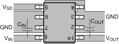 Figure 23. LM2936BM SOIC (D) Layout
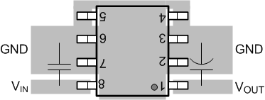 Figure 24. LM2936M SOIC (D) Layout
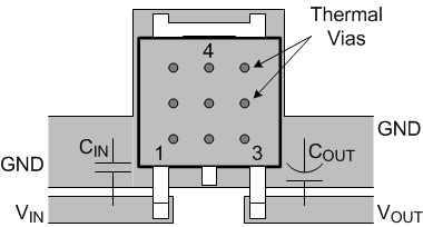 Figure 25. LM2936 TO-252 (NDP) Layout
10.3 Thermal Considerations
Due to the power dissipation characteristics of the available packages (RθJA), full output current cannot be ensured for all combinations of ambient temperature and input voltage.
Exceeding the maximum allowable power dissipation as defined by the final package RθJA will cause excessive die junction temperature, and the regulator may go into thermal shutdown.
Power dissipation, PD, is calculated from the following formula:
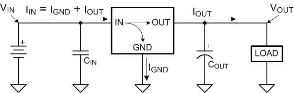 Figure 26. Current Paths for Power Dissipation Calculation
Knowing the power dissipation (PD), the thermal resistance of the package (RθJA), and the ambient temperature (TA), the junction temperature (TJ) can be estimated using the following formula:
Knowing the thermal resistance of the package (RθJA), the ambient temperature (TA), and the maximum allowed operating junction temperature (TJ) of 125°C, the maximum power dissipation can be estimated using the following formula:
Alternately, solving for the required thermal resistance (RθJA):
The maximum allowed PD information from Equation 3 can be used to estimate the maximum allowed load current (IOUT), or the maximum allowed VIN:
As an example, an application requires : VIN = 14 V, VOUT = 5 V, IOUT = 25 mA, and TA = 85°C. Find the maximum RθJA to keep the junction temperature under 125°C.
The EIA/JEDEC standard (JESD51-2) provides methodologies to estimate the junction temperature from external measurements (ΨJB references the temperature at the PCB, and ΨJT references the temperature at the top surface of the package) when operating under steady-state power dissipation conditions. These methodologies have been determined to be relatively independent of the copper thermal spreading area that may be attached to the package DAP when compared to the more typical RθJA. Refer to Texas Instruments Application Report Semiconductor and IC Package Thermal Metrics (SPRA953), for specifics.
On the 8-pin SOIC (D) package, the four ground pins are thermally connected to the backside of the die. Adding approximately 0.04 square inches of 2 oz. copper pad area to these four pins will improve the JEDEC RθJA rating from 111.4°C/W to approximately 100°C/W. If this extra copper area is placed directly beneath the SOIC package there should not be any impact on board density.
The LM2936 has an internally set thermal shutdown point of typically 160°C. Thermal shutdown is outside the ensured operating temperature range and is intended as a safety feature only. Continuous operation near the thermal shutdown temperature should be avoided as it may have a negative affect on the life of the device.