SNVS769J March 2000 – December 2014 LM2940-N , LM2940C
PRODUCTION DATA.
- 1 Features
- 2 Applications
- 3 Description
- 4 Revision History
- 5 Pin Configuration and Functions
- 6 Specifications
- 7 Detailed Description
- 8 Application and Implementation
- 9 Power Supply Recommendations
- 10Layout
- 11Device and Documentation Support
- 12Mechanical, Packaging, and Orderable Information
デバイスごとのパッケージ図は、PDF版データシートをご参照ください。
メカニカル・データ(パッケージ|ピン)
- NDE|3
- NGN|8
- DCY|4
- KTT|3
- NEB|3
サーマルパッド・メカニカル・データ
- KTT|3
7 Detailed Description
7.1 Overview
The LM2940 positive voltage regulator features the ability to source 1 A of output current with a dropout voltage of typically 0.5 V and a maximum of 1 V over the entire temperature range. Furthermore, a quiescent current reduction circuit has been included which reduces the ground current when the differential between the input voltage and the output voltage exceeds approximately 3 V. The quiescent current with 1 A of output current and an input-output differential of 5 V is therefore only 30 mA. Higher quiescent currents only exist when the regulator is in the dropout mode (VIN – VOUT ≤ 3 V).
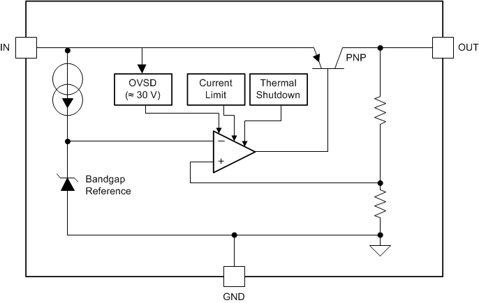
7.2 Functional Block Diagram
7.3 Feature Description
7.3.1 Short-Circuit Current Limit
The internal current limit circuit is used to protect the LDO against high-load current faults or shorting events. The LDO is not designed to operate in a steady-state current limit. During a current-limit event, the LDO sources constant current. Therefore, the output voltage falls when load impedance decreases. Note, also, that if a current limit occurs and the resulting output voltage is low, excessive power may be dissipated across the LDO, resulting a thermal shutdown of the output.
7.3.2 Overvoltage Shutdown (OVSD)
Input voltage greater than typically 30 V will cause the LM2940 output to be disabled. When operating with the input voltage greater than the maximum recommended input voltage of 26 V, the device performance is not ensured. Continuous operation with the input voltage greater than the maximum recommended input voltage is discouraged.
7.3.3 Thermal Shutdown (TSD)
The LM2940 contains the thermal shutdown circuitry to turn off the output when excessive heat is dissipated in the LDO. The internal protection circuitry of the LM2940 is designed to protect against thermal overload conditions. The TSD circuitry is not intended to replace proper heat sinking. Continuously running the device into thermal shutdown degrades its reliability as the junction temperature will be exceeding the absolute maximum junction temperature rating.
7.4 Device Functional Modes
7.4.1 Operation with Enable Control
The LM2940 design does not include any undervoltage lockout (UVLO), or enable functions. Generally, the output voltage will track the input voltage until the input voltage is greater than VOUT + 1V. When the input voltage is greater than VOUT + 1 V, the LM2940 will be in linear operation, and the output voltage will be regulated. However, the device will be sensitive to any small perturbation of the input voltage. Device dynamic performance is improved when the input voltage is at least 2 V greater than the output voltage.