SNOS935C February 2001 – December 2014 LM321
PRODUCTION DATA.
- 1 Features
- 2 Applications
- 3 Description
- 4 Revision History
- 5 Pin Configuration and Functions
- 6 Specifications
- 7 Detailed Description
- 8 Application and Implementation
- 9 Power Supply Recommendations
- 10Layout
- 11Device and Documentation Support
- 12Mechanical, Packaging, and Orderable Information
8 Application and Implementation
NOTE
Information in the following applications sections is not part of the TI component specification, and TI does not warrant its accuracy or completeness. TI’s customers are responsible for determining suitability of components for their purposes. Customers should validate and test their design implementation to confirm system functionality.
8.1 Application Information
The LM321 operational amplifer can operate with a single or dual power supply voltage, has true-differential inputs, and remain in the linear mode with an input common-mode voltage of 0 VDC. This amplifier operates over a wide range of power supply voltages, with little change in performance characteristics. At 25°C amplifier operation is possible down to a minimum supply voltage of 3 V.
Large differential input voltages can be easily accommodated and, as input differential voltage protection diodes are not needed, no large input currents result from large differential input voltages. The differential input voltage may be larger than V+ without damaging the device. Protection should be provided to prevent the input voltages from going negative more than −0.3 VDC (at 25°C).An input clamp diode with a resistor to the IC input terminal can be used.
To reduce the power supply drain, the amplifier has a class A output stage for small signal levels which converts to class B in a large signal mode. This allows the amplifiers to both source and sink large output currents. Therefore both NPN and PNP external current boost transistors can be used to extend the power capability of the basic amplifiers. The output voltage needs to raise approximately 1 diode drop above ground to bias the on-chip vertical PNP transistor for output current sinking applications.
For AC applications, where the load is capacitively coupled to the output of the amplifier, a resistor should be used, from the output of the amplifier to ground to increase the class A bias current and to reduce distortion.
Capacitive loads which are applied directly to the output of the amplifier reduce the loop stability margin. Values of 50pF can be accommodated using the worst-case non-inverting unity gain connection. Large closed loop gains or resistive isolation should be used if large load capacitance must be driven by the amplifier.
The bias network of the LM321 establishes a supply current which is independent of the magnitude of the power supply voltage over the range of from 3 VDC to 30 VDC.
Output short circuits either to ground or to the positive power supply should be of short time duration. Units can be destroyed, not as a result of the short circuit current causing metal fusing, but rather due to the large increase in IC chip dissipation which will cause eventual failure due to excessive junction temperatures. The larger value of output source current which is available at 25°C provides a larger output current capability at elevated temperatures than a standard IC operational amplifer.
The circuits presented in the section on typical applications emphasize operation on only a single power supply voltage. If complementary power supplies are available, all of the standard operational amplifer circuits can be used. In general, introducing a pseudo-ground (a bias voltage reference of V+/2) will allow operation above and below this value in single power supply systems. Many application circuits are shown which take advantage of the wide input common-mode voltage range which includes ground. In most cases, input biasing is not required and input voltages which range to ground can easily be accommodated.
8.2 Typical Applications
8.2.1 Noninverting DC Gain (0-V Input = 0-V Output)
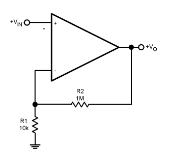 Figure 7. Non-Inverting DC Gain Schematic (0-V Input = 0-V Output)
8.2.1.1 Design Requirements
- Supply voltage (up to 32 V)
- Phase margin: 60°
8.2.1.2 Detailed Design Procedure
- Connect 1-MΩ feedback resistor between the output and the inverting terminal of the amplifier.
- Connect 10-kΩ resistor between the inverting terminal and ground. Place the resistor as close to the inverting pin as possible.
- Connect power supply and input voltages.
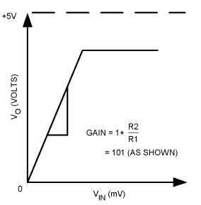
8.2.1.3 Application Curve
8.2.2 DC Summing Amplifier (VIN's ≥ 0 VDC and VO ≥ VDC)
The summing amplifier, a special case of the inverting amplifier, is shown in Figure 7. The circuit gives an inverted output which is equal to the weighted algebraic sum of all four inputs. The gain of any input of this circuit is equal to the ratio of the appropriate input resistor to the feedback resistor. The advantage of this circuit is that there is no interaction between inputs and operations such as summing and weighted averaging are implemented very easily.
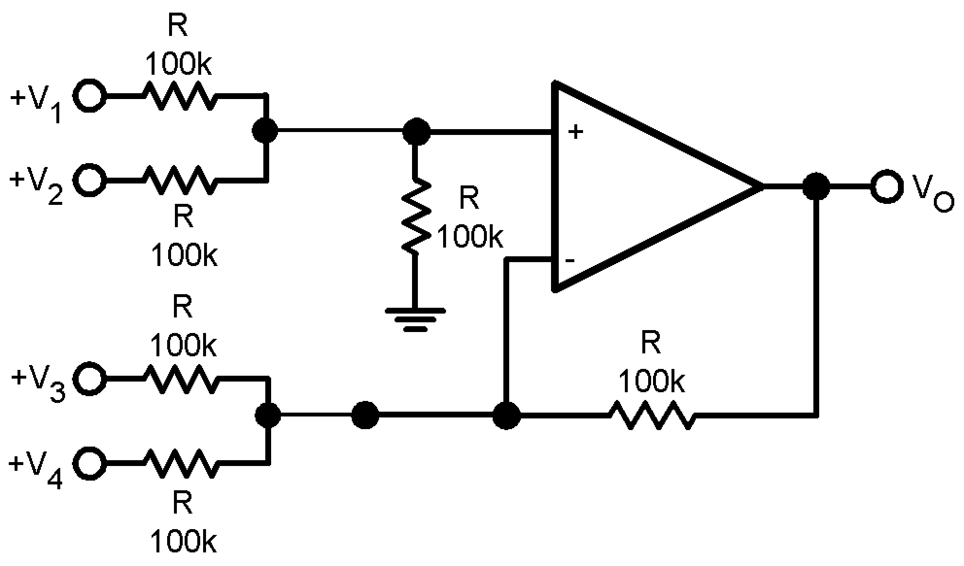
(VIN's ≥ 0 VDC and VO ≥ VDC)
8.2.3 Amplitude Modulator Circuit
The modulator circuit is shown in Figure 10. PWM signal is used to switch the MOSFET. When the MOSFET is on, the circuit acts as an inverting amplifier with gain 1. When The MOSFET is off, the inverting and non-inverting signals cancel each other out. Therefore, the output switches from –VIN to GND at the carrier frequency.
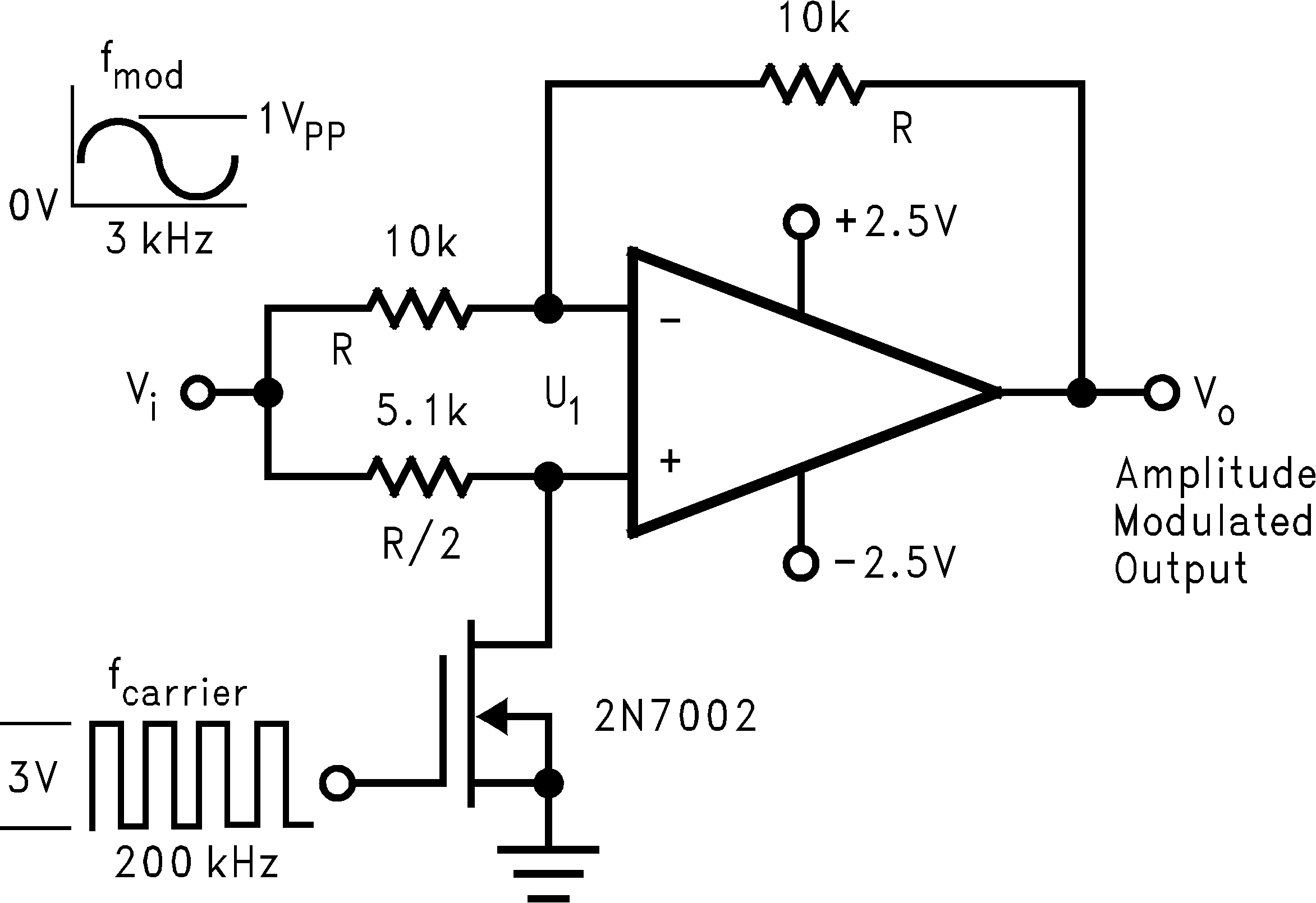 Figure 10. Amplitude Modulator Circuit Schematic
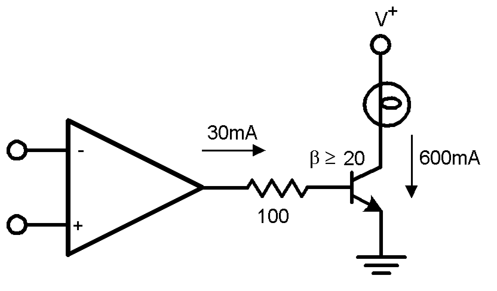
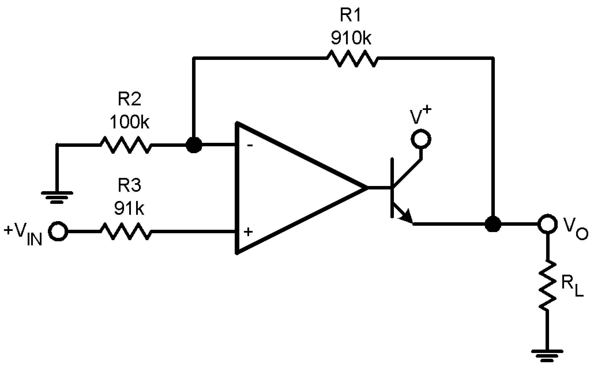
8.2.4 Power Amplifier
Power amplifier application circuit is shown in Figure 11. Voltage gain is set by R1 and R2. The output of the amplifier is connected to the base of BJT which amplifies the current. Current gain is set by β, current gain of a BJT. The resulting output provides high power to the load. Differential voltage supplies are necessary.
8.2.5 LED Driver
LM321 operating as an LED driver is shown in Figure 12. The output of the amplifier sets the current through the diode. The voltage across the LED is assumed constant.
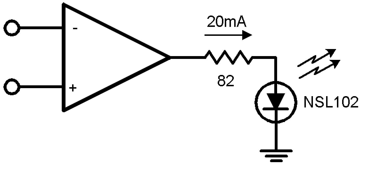 Figure 12. LED Driver Schematic
8.2.6 Fixed Current Sources
Operational amplifier can be used to provide fixed current source to multiple loads. The output voltage of the amplifier is connected to bases of bipolar transistors. The feedback is provided from the drain of a BJT to the inverting terminal of the amplifier. Currents in the second and later BJTs are set by the ratio of R1 and R2.
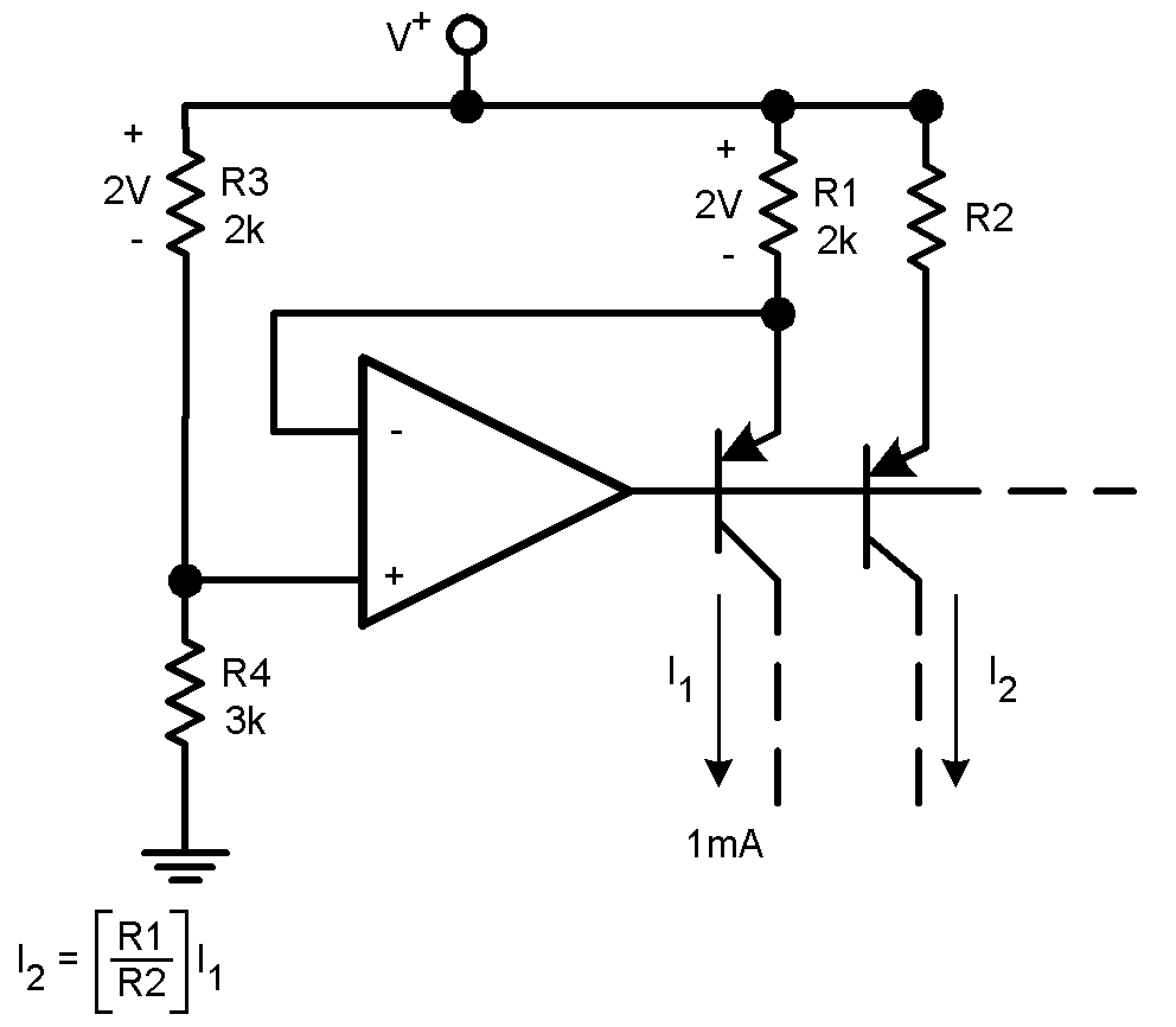 Figure 13. Fixed Current Sources Schematic