SNVS846G June 2012 – November 2017 LM34925
PRODUCTION DATA.
- 1 Features
- 2 Applications
- 3 Description
- 4 Revision History
- 5 Pin Configuration and Functions
- 6 Specifications
-
7 Detailed Description
- 7.1 Overview
- 7.2 Functional Block Diagram
- 7.3
Feature Description
- 7.3.1 Control Overview
- 7.3.2 VCC Regulator
- 7.3.3 Regulation Comparator
- 7.3.4 Overvoltage Comparator
- 7.3.5 On-Time Generator
- 7.3.6 Current Limit
- 7.3.7 N-Channel Buck Switch and Driver
- 7.3.8 Synchronous Rectifier
- 7.3.9 Undervoltage Detector
- 7.3.10 Thermal Protection
- 7.3.11 Ripple Configuration
- 7.3.12 Soft Start
- 7.4 Device Functional Modes
-
8 Application and Implementation
- 8.1 Application Information
- 8.2
Typical Application
- 8.2.1
Application Circuit: 20-V to 95-V Input and 10-V, 100-mA Output Isolated Fly-Buck Converter
- 8.2.1.1 Design Requirements
- 8.2.1.2
Detailed Design Procedure
- 8.2.1.2.1 Transformer Turns Ratio
- 8.2.1.2.2 Total IOUT
- 8.2.1.2.3 RFB1, RFB2
- 8.2.1.2.4 Frequency Selection
- 8.2.1.2.5 Transformer Selection
- 8.2.1.2.6 Primary Output Capacitor
- 8.2.1.2.7 Secondary Output Capacitor
- 8.2.1.2.8 Type III Feedback Ripple Circuit
- 8.2.1.2.9 Secondary Diode
- 8.2.1.2.10 VCC and Bootstrap Capacitor
- 8.2.1.2.11 Input Capacitor
- 8.2.1.2.12 UVLO Resistors
- 8.2.1.2.13 VCC Diode
- 8.2.2 Application Curves
- 8.2.1
Application Circuit: 20-V to 95-V Input and 10-V, 100-mA Output Isolated Fly-Buck Converter
- 9 Power Supply Recommendations
- 10Layout
- 11Device and Documentation Support
- 12Mechanical, Packaging, and Orderable Information
パッケージ・オプション
メカニカル・データ(パッケージ|ピン)
サーマルパッド・メカニカル・データ
- DDA|8
発注情報
10 Layout
10.1 Layout Guidelines
A proper layout is essential for optimum performance of the circuit. In particular, the following guidelines should be observed:
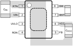
- CIN: The loop consisting of input capacitor (CIN), VIN pin, and RTN pin carries switching currents. Therefore the input capacitor should be placed close to the IC, directly across VIN and RTN pins and the connections to these two pins should be direct to minimize the loop area. In general it is not possible to accommodate all of input capacitance near the IC. A good practice is to use a 0.1-μF or 0.47-μF capacitor directly across the VIN and RTN pins close to the IC, and the remaining bulk capacitor as close as possible (see Figure 18).
- CVCC and CBST: The VCC and bootstrap (BST) bypass capacitors supply switching currents to the high and low-side gate drivers. These two capacitors should also be placed as close to the IC as possible, and the connecting trace lengths and loop area should be minimized (see Figure 18).
- The Feedback trace carries the output voltage information and a small ripple component that is necessary for proper operation of LM34925. Therefore care should be taken while routing the feedback trace so avoid coupling any noise to this pin. In particular, feedback trace should not run close to magnetic components, or parallel to any other switching trace.
- SW trace: SW node switches rapidly between VIN and GND every cycle and is therefore a possible source of noise. SW node area should be minimized. In particular SW node should not be inadvertently connected to a copper plane or pour.
10.2 Layout Example
 Figure 18. Placement of Bypass Capacitors