SNVS847F June 2012 – November 2017 LM34926
PRODUCTION DATA.
- 1 Features
- 2 Applications
- 3 Description
- 4 Revision History
- 5 Pin Configuration and Functions
- 6 Specifications
-
7 Detailed Description
- 7.1 Overview
- 7.2 Functional Block Diagram
- 7.3
Feature Description
- 7.3.1 Control Overview
- 7.3.2 VCC Regulator
- 7.3.3 Regulation Comparator
- 7.3.4 Overvoltage Comparator
- 7.3.5 On-Time Generator
- 7.3.6 Current Limit
- 7.3.7 N-Channel Buck Switch and Driver
- 7.3.8 Synchronous Rectifier
- 7.3.9 Undervoltage Detector
- 7.3.10 Thermal Protection
- 7.3.11 Ripple Configuration
- 7.3.12 Soft Start
- 7.4 Device Functional Modes
-
8 Application and Implementation
- 8.1 Application Information
- 8.2
Typical Application
- 8.2.1 Design Requirements
- 8.2.2
Detailed Design Procedure
- 8.2.2.1 Custom Design With WEBENCH® Tools
- 8.2.2.2 Transformer Turns Ratio
- 8.2.2.3 Total IOUT
- 8.2.2.4 RFB1, RFB2
- 8.2.2.5 Frequency Selection
- 8.2.2.6 Transformer Selection
- 8.2.2.7 Primary Output Capacitor
- 8.2.2.8 Secondary Output Capacitor
- 8.2.2.9 Type III Feedback Ripple Circuit
- 8.2.2.10 Secondary Diode
- 8.2.2.11 VCC and Bootstrap Capacitor
- 8.2.2.12 Input Capacitor
- 8.2.2.13 UVLO Resistors
- 8.2.2.14 VCC Diode
- 8.2.3 Application Curves
- 9 Power Supply Recommendations
- 10Layout
- 11Device and Documentation Support
- 12Mechanical, Packaging, and Orderable Information
パッケージ・オプション
メカニカル・データ(パッケージ|ピン)
サーマルパッド・メカニカル・データ
- DDA|8
発注情報
6 Specifications
6.1 Absolute Maximum Ratings(1)(2)
| MIN | MAX | UNIT | |
|---|---|---|---|
| VIN, UVLO to RTN | –0.3 | 100 | V |
| SW to RTN | –1.5 | VIN + 0.3 | V |
| SW to RTN (100-ns transient) | –5 | VIN + 0.3 | V |
| BST to VCC | 100 | V | |
| BST to SW | 13 | V | |
| RON to RTN | –0.3 | 100 | V |
| VCC to RTN | –0.3 | 13 | V |
| FB to RTN | –0.3 | 5 | V |
| Maximum junction temperature(3) | 150 | °C | |
| Storage temperature, Tstg | –55 | 150 | °C |
(1) Stresses beyond those listed under Absolute Maximum Ratings may cause permanent damage to the device. These are stress ratings only, which do not imply functional operation of the device at these or any other conditions beyond those indicated under Recommended Operating Conditions. Exposure to absolute-maximum-rated conditions for extended periods may affect device reliability.
(2) The RTN pin is the GND reference electrically connected to the substrate.
(3) High junction temperatures degrade operating lifetimes. Operating lifetime is derated for junction temperatures greater than 125°C.
6.2 ESD Ratings
| VALUE | UNIT | |||
|---|---|---|---|---|
| V(ESD) | Electrostatic discharge | Human-body model (HBM), per ANSI/ESDA/JEDEC JS-001(1) | ±2000 | V |
| Charged-device model (CDM), per JEDEC specification JESD22-C101(2) | ±750 | |||
(1) JEDEC document JEP155 states that 500-V HBM allows safe manufacturing with a standard ESD control process.
(2) JEDEC document JEP157 states that 250-V CDM allows safe manufacturing with a standard ESD control process.
6.3 Recommended Operating Ratings
| MIN | MAX | UNIT | |
|---|---|---|---|
| VIN voltage | 7.5 | 100 | V |
| Operating junction temperature(1) | –40 | 125 | °C |
(1) High junction temperatures degrade operating lifetimes. Operating lifetime is derated for junction temperatures greater than 125°C.
6.4 Thermal Information
| THERMAL METRICS(1) | LM34926 | UNIT | |||
|---|---|---|---|---|---|
| NGU (WSON) | DDA (SO PowerPAD) | ||||
| 8 PINS | 8 PINS | ||||
| RθJA | Junction-to-ambient thermal resistance | 41.3 | 41.1 | °C/W | |
| RθJC(bot) | Junction-to-case (bottom) thermal resistance | 3.2 | 2.4 | °C/W | |
| ΨJB | Junction-to-board thermal characteristic parameter | 19.2 | 24.4 | °C/W | |
| RθJB | Junction-to-board thermal resistance | 19.1 | 30.6 | °C/W | |
| RθJC(top) | Junction-to-case (top) thermal resistance | 34.7 | 37.3 | °C/W | |
| ΨJT | Junction-to-top thermal characteristic parameter | 0.3 | 6.7 | °C/W | |
(1) For more information about traditional and new thermal metrics, see the IC Package Thermal Metrics application report (SPRA953).
6.5 Electrical Characteristics
Typical values correspond to TJ = 25°C. Minimum and maximum limits apply over –40°C to 125°C junction temperature range unless otherwise stated. VIN = 48 V unless stated otherwise. See(1).| PARAMETER | TEST CONDITIONS | MIN | TYP | MAX | UNIT | |
|---|---|---|---|---|---|---|
| VCC SUPPLY | ||||||
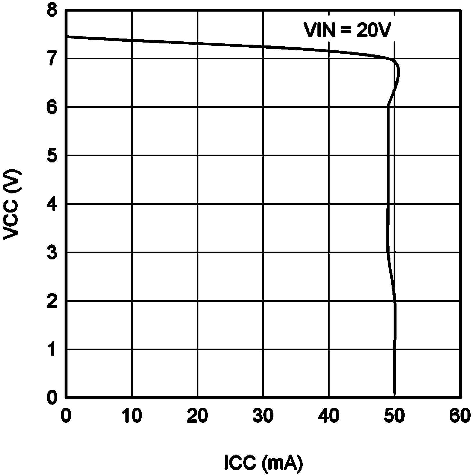
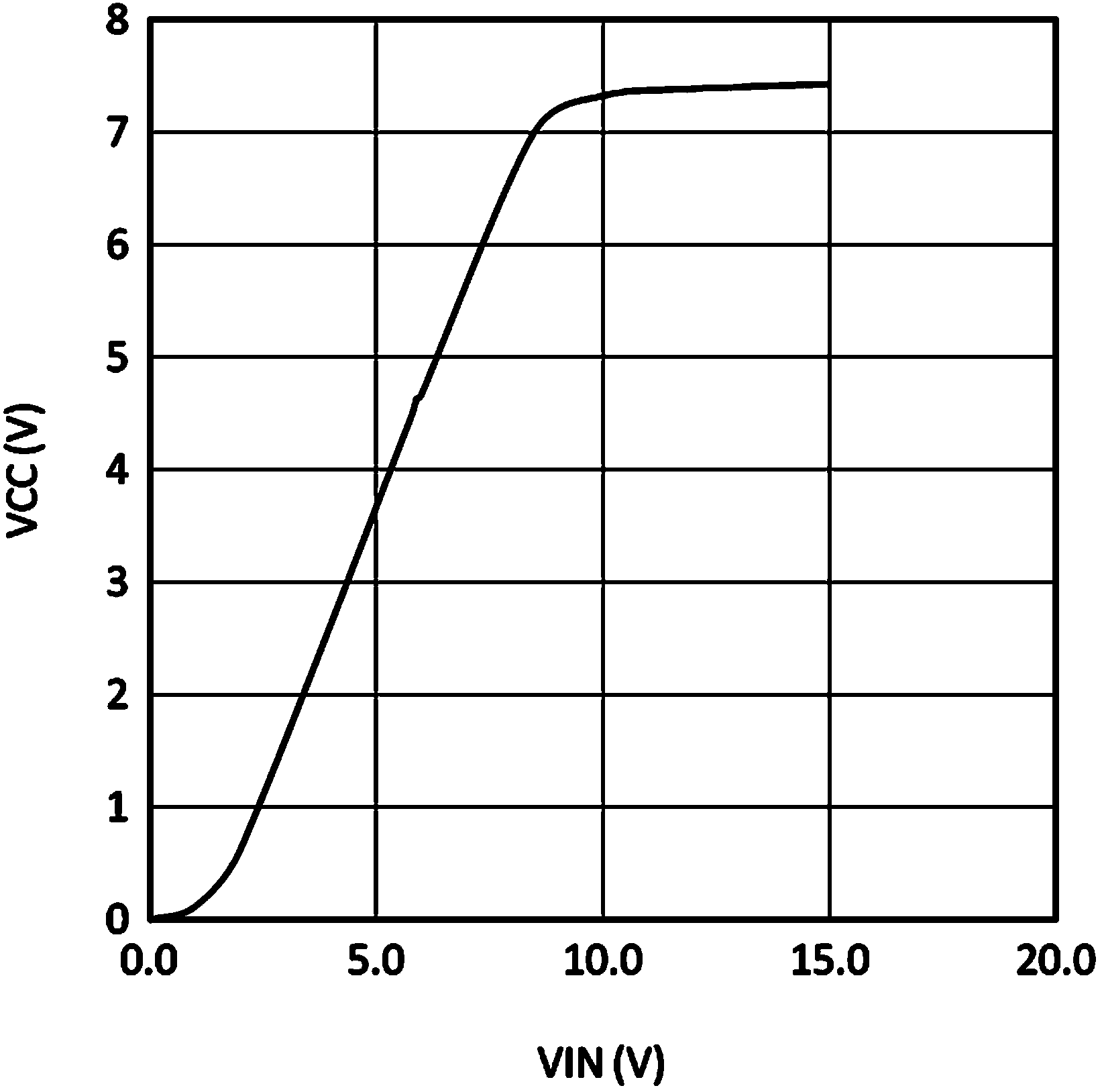
| VCC Reg | VCC Regulator Output | VIN = 48 V, ICC = 20 mA | 6.25 | 7.6 | 8.55 | V |
| VCC Current Limit | VIN = 48 V(2) | 26 | mA | |||
| VCC UVLO Threshold (VCC increasing) | 4.15 | 4.5 | 4.9 | V | ||
| VCC UVLO Hysteresis | 300 | mV | ||||
| VCC Drop Out Voltage | VIN = 8 V, ICC = 20 mA | 2.3 | V | |||
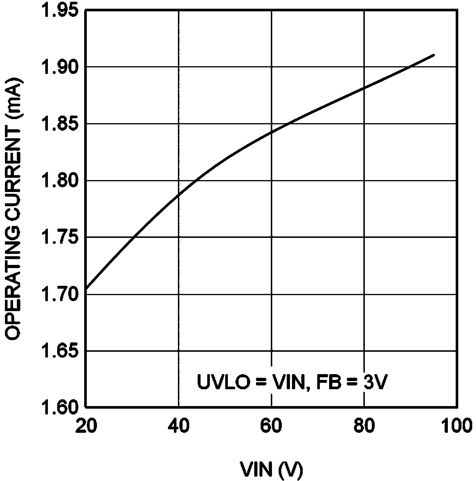
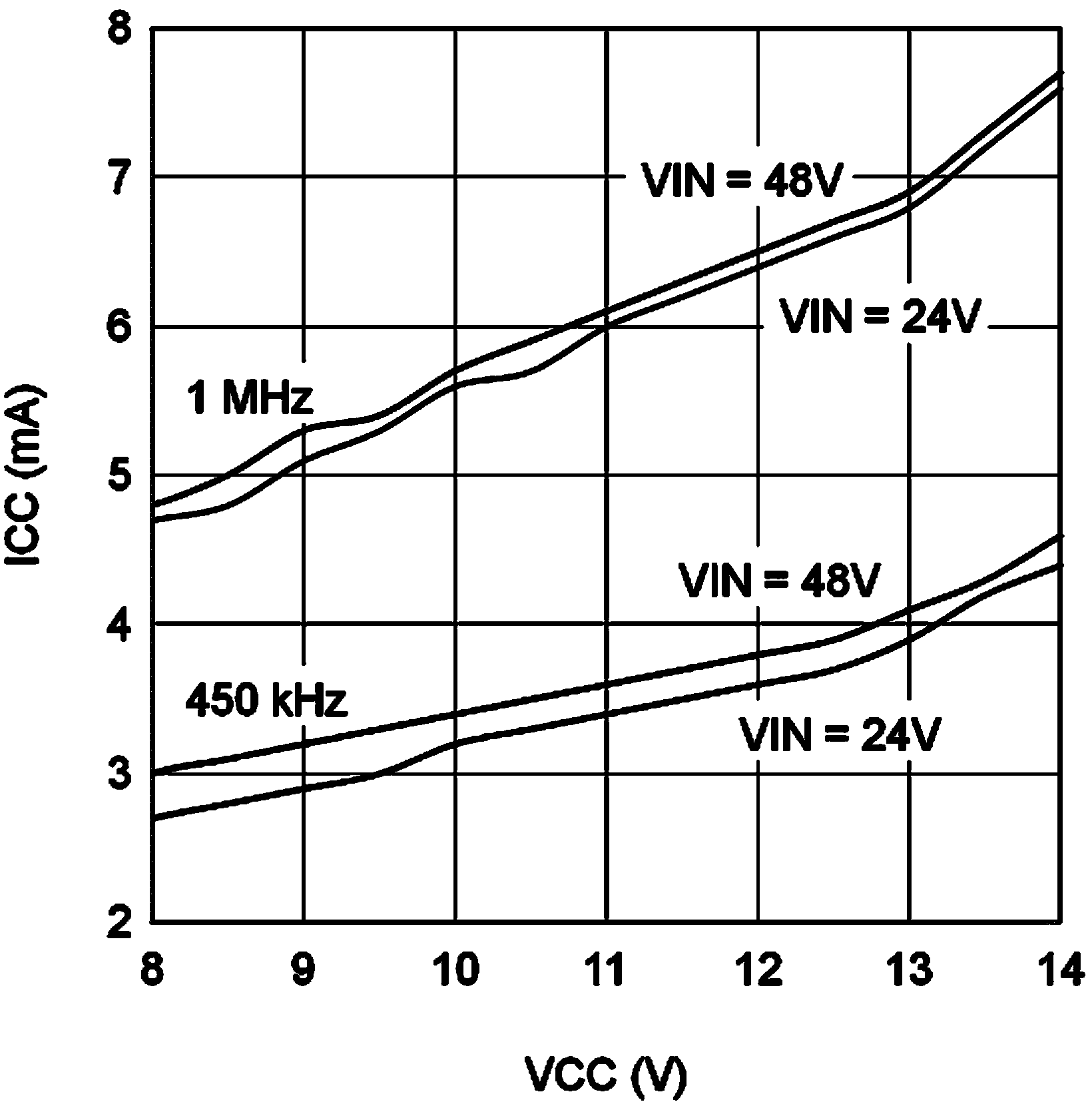
| IIN Operating Current | Nonswitching, FB = 3 V | 1.75 | mA | |||
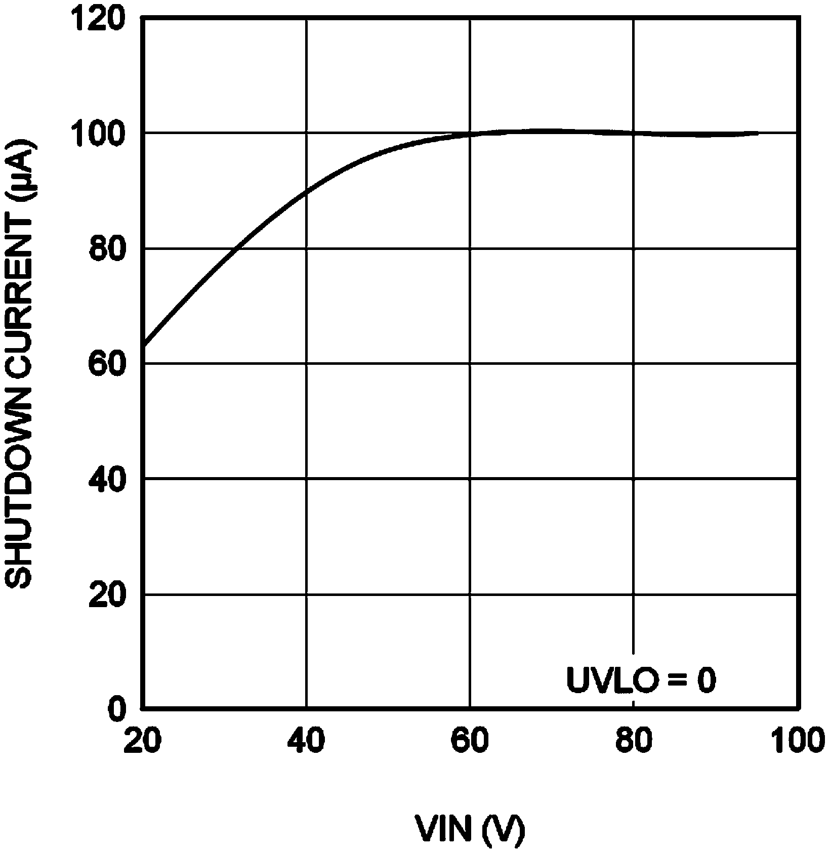
| IIN Shutdown Current | UVLO = 0 V | 50 | 225 | µA | ||
| UNDERVOLTAGE SENSING FUNCTION | ||||||
| UV Threshold | UV Rising | 1.19 | 1.225 | 1.26 | V | |
| UV Hysteresis Input Current | UV = 2.5 V | –10 | –20 | -29 | µA | |
| Remote Shutdown Threshold | Voltage at UVLO Falling | 0.32 | 0.66 | V | ||
| Remote Shutdown Hysteresis | 110 | mV | ||||
| REGULATION AND OVERVOLTAGE COMPARATORS | ||||||
| FB Regulation Level | Internal Reference Trip Point for Switch ON | 1.2 | 1.225 | 1.25 | V | |
| FB Overvoltage Threshold | Trip Point for Switch OFF | 1.62 | V | |||
| FB Bias Current | 60 | nA | ||||
| SWITCH CHARACTERISTICS | ||||||
| Buck Switch RDS(ON) | ITEST = 200 mA, BST-SW = 7 V | 0.8 | 1.8 | Ω | ||
| Synchronous RDS(ON) | ITEST = 200 mA | 0.45 | 1 | Ω | ||
| Gate Drive UVLO | VBST − VSW Rising | 2.4 | 3 | 3.6 | V | |
| Gate Drive UVLO Hysteresis | 260 | mV | ||||
| CURRENT LIMIT | ||||||
| Current Limit Threshold | 390 | 575 | 750 | mA | ||
| Current Limit Response Time | Time to Switch Off | 150 | ns | |||
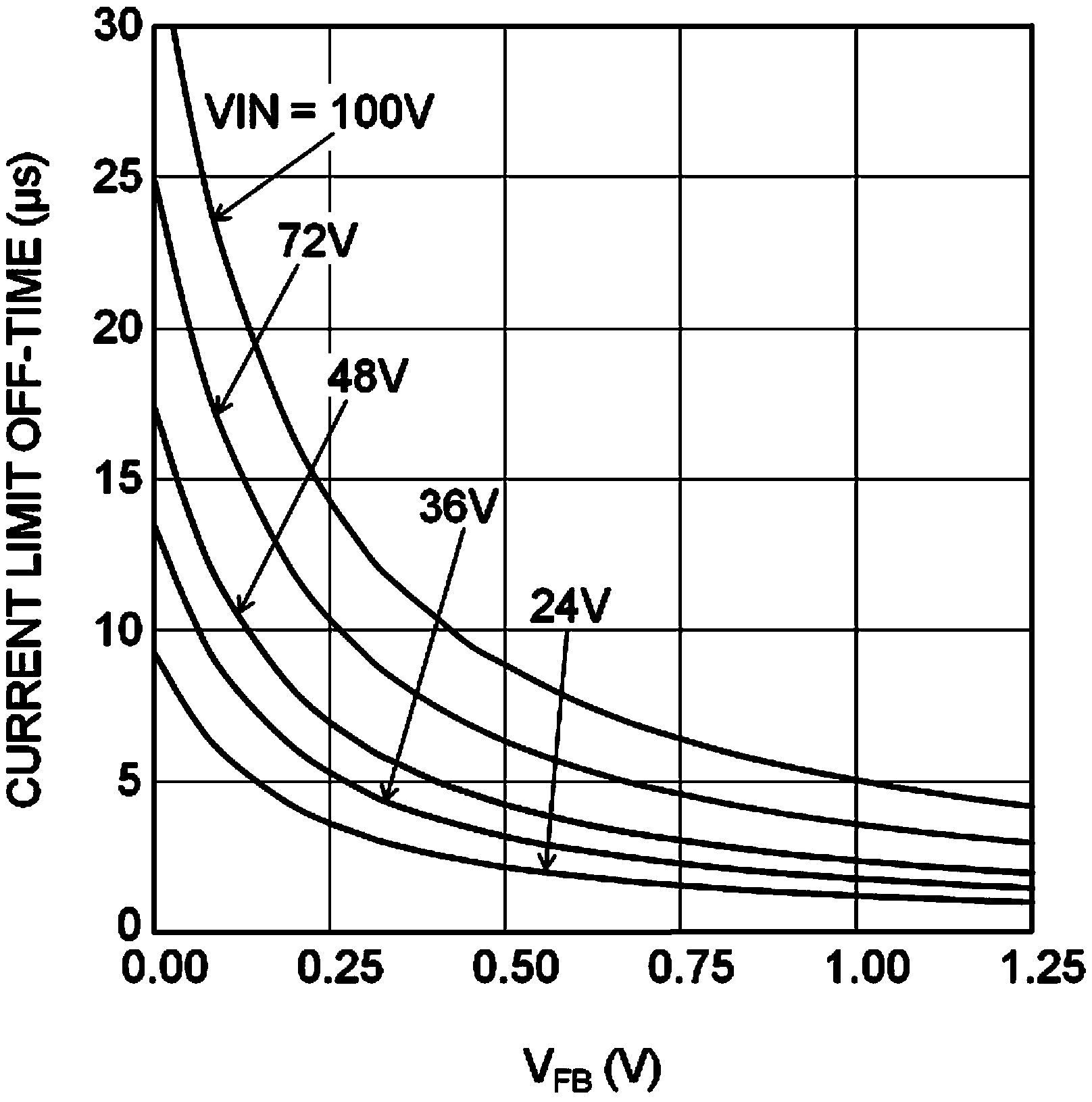
| OFF-Time Generator (Test 1) | FB = 0.1 V, VIN = 48 V | 12 | µs | |||
| OFF-Time Generator (Test 2) | FB = 1.0 V, VIN = 48 V | 2.5 | µs | |||
| THERMAL SHUTDOWN | ||||||
| Tsd | Thermal Shutdown Temperature | 165 | °C | |||
| Thermal Shutdown Hysteresis | 20 | °C | ||||
(1) All limits are specified by design. All electrical characteristics having room temperature limits are tested during production at TA = 25°C. All hot and cold limits are ensured by correlating the electrical characteristics to process and temperature variations and applying statistical process control.
(2) VCC provides self bias for the internal gate drive and control circuits. Device thermal limitations limit external loading.
6.6 Switching Characteristics
Typical values correspond to TJ = 25°C. Minimum and maximum limits apply over –40°C to 125°C junction temperature range unless otherwise stated. VIN = 48 V unless otherwise stated.| MIN | TYP | MAX | UNIT | |||
|---|---|---|---|---|---|---|
| ON-TIME GENERATOR | ||||||
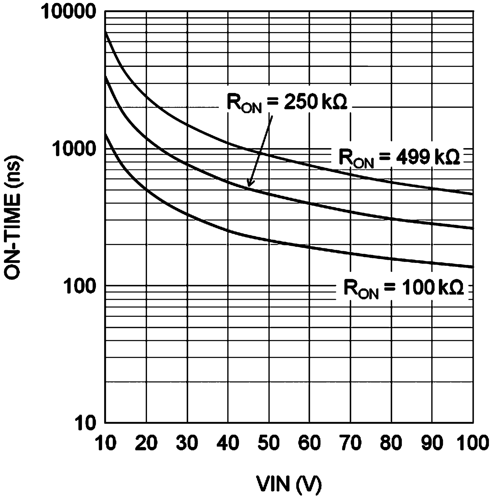
| TON Test 1 | VIN = 32 V, RON = 100 kΩ | 270 | 350 | 460 | ns | |
| TON Test 2 | VIN = 48 V, RON = 100 kΩ | 188 | 250 | 336 | ns | |
| TON Test 3 | VIN = 75 V, RON = 250 kΩ | 250 | 370 | 500 | ns | |
| TON Test 4 | VIN = 10 V, RON = 250 kΩ | 1880 | 3200 | 4425 | ns | |
| MINIMUM OFF-TIME | ||||||
| Minimum Off-Timer | FB = 0 V | 144 | ns | |||
