JAJSAO5I January 2007 – December 2017 LM5022
PRODUCTION DATA.
- 1 特長
- 2 アプリケーション
- 3 概要
- 4 改訂履歴
- 5 Pin Configuration and Functions
- 6 Specifications
- 7 Detailed Description
-
8 Application and Implementation
- 8.1 Application Information
- 8.2
Typical Application
- 8.2.1 Design Requirements
- 8.2.2
Detailed Design Procedure
- 8.2.2.1 Switching Frequency
- 8.2.2.2 MOSFET
- 8.2.2.3 Output Diode
- 8.2.2.4 Boost Inductor
- 8.2.2.5 Output Capacitor
- 8.2.2.6 VCC Decoupling Capacitor
- 8.2.2.7 Input Capacitor
- 8.2.2.8 Current Sense Filter
- 8.2.2.9 RSNS, RS2 and Current Limit
- 8.2.2.10 Control Loop Compensation
- 8.2.2.11 Efficiency Calculations
- 8.2.3 Application Curves
- 9 Power Supply Recommendations
- 10Layout
- 11デバイスおよびドキュメントのサポート
- 12メカニカル、パッケージ、および注文情報
7.3.2 Input Undervoltage Detector
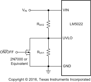
The LM5022 contains an input undervoltage lockout (UVLO) circuit. UVLO is programmed by connecting the UVLO pin to the center point of an external voltage divider from VIN to GND. The resistor divider must be designed such that the voltage at the UVLO pin is greater than 1.25 V when VIN is in the desired operating range. If the undervoltage threshold is not met, all functions of the controller are disabled and the controller remains in a low power standby state. UVLO hysteresis is accomplished with an internal 20-µA current source that is switched on or off into the impedance of the setpoint divider. When the UVLO threshold is exceeded, the current source is activated to instantly raise the voltage at the UVLO pin. When the UVLO pin voltage falls below the 1.25-V threshold the current source is turned off, causing the voltage at the UVLO pin to fall. The UVLO pin can also be used to implement a remote enable or disable function. If an external transistor pulls the UVLO pin below the 1.25-V threshold, the converter is disabled. This external shutdown method is shown in Figure 11.
 Figure 11. Enable or Disable Using UVLO